A Schottky diode-based millimeter wave overprotection circuit and its preparation method

A Schottky diode and over-protection technology, applied in the field of microelectronics, which can solve the problem that it cannot meet the needs of higher frequency and higher power electronic devices, and the ability of the Schottky barrier limiter to impact high-power signals is not strong enough and other problems, to achieve the effect of reducing the gate-drain parasitic capacitance and reducing the frequency loss

Active Publication Date: 2020-12-29
XIDIAN UNIV
View PDF5 Cites 0 Cited by
  • Summary
  • Abstract
  • Description
  • Claims
  • Application Information

AI Technical Summary

Problems solved by technology

[0005] However, the second-generation gallium arsenide semiconductor material cannot meet the needs of higher frequency and higher power electronic devices, and the ability of the Schottky barrier limiter to withstand the impact of high power signals in the same area is not strong enough, and the disadvantages are more obvious.

Method used


Image

  • A Schottky diode-based millimeter wave overprotection circuit and its preparation method
  • A Schottky diode-based millimeter wave overprotection circuit and its preparation method

Examples


Embodiment 1

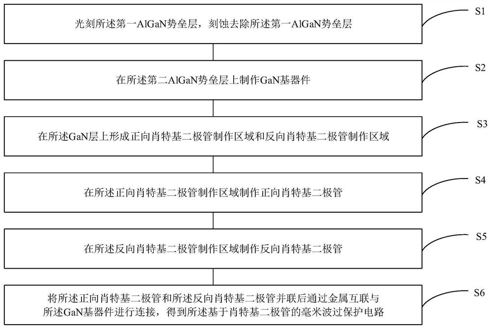
[0051] See figure 1 , figure 1It is a schematic process flow diagram of a Schottky diode-based millimeter wave overprotection circuit manufacturing method provided by an embodiment of the present invention. A method for preparing a Schottky diode-based millimeter-wave overprotection circuit, applied to an AlGaN / GaN heterojunction, the AlGaN / GaN heterojunction comprising a substrate layer, a nucleation layer, a GaN layer, and a first AlGaN barrier layer, a second AlGaN barrier layer, wherein the method comprises:

[0052] S1. Photoetching the first AlGaN barrier layer, and etching and removing the first AlGaN barrier layer;

[0053] The AlGaN / GaN heterojunction material is obtained and cleaned, and the first AlGaN barrier layer is removed by ICP dry etching.

[0054] First place the disc in acetone for 2 minutes, then boil it in a positive glue stripping solution heated in a water bath at 60°C for 10 minutes, then place the sample in acetone and ethanol for 3 minutes each, a...


PUM

PropertyMeasurementUnit
widthaaaaaaaaaa
thicknessaaaaaaaaaa
thicknessaaaaaaaaaa

Abstract

The invention relates to a preparation method of a millimeter wave overprotection circuit based on a Schottky diode, comprises manufacturing a forward Schottky diode, a reverse Schottky diode and a GaN-based device, connecting the forward Schottky diode and the reverse Schottky diode in parallel with each other and connecting the forward Schottky diode and the reverse Schottky diode with the GaN-based device through a metal interconnection process, thereby completing the fabrication of a millimeter wave overprotection circuit based on the Schottky diode. In the embodiment of the invention, byadopting a circuit in which a forward Schottky diode and a reverse Schottky diode are connected in parallel with the gate of a GaN-based device, self-protection of the circuit can be realized, and atthe same time, the device can withstand the impact of the forward and reverse high-power signals, and bi-directional protection of the device can be realized.

Description

technical field [0001] The invention belongs to the technical field of microelectronics, and in particular relates to a Schottky diode-based millimeter wave overprotection circuit and a preparation method thereof. Background technique [0002] With the continuous advancement of semiconductor technology, silicon-based semiconductor technology has achieved continuous development for decades and has become the most mature technology in today's semiconductor technology. However, in the field of power semiconductors, silicon-based devices are approaching their theoretical limits. First, The second-generation semiconductor materials can no longer meet the needs of higher frequency and higher power electronic devices. The research on new semiconductor material devices is particularly important. Electronic devices based on nitride semiconductor materials can meet this requirement and greatly improve device performance. [0003] Monolithic microwave integrated circuit is an integrate...

Claims


Application Information

Patent Timeline
Patent Type & Authority Patents(China)
IPC IPC(8): H01L21/8252H01L27/08
CPCH01L21/8252H01L27/0814
Inventor 杨凌马晓华芦浩侯斌宓珉翰祝杰杰周小伟郝跃
Owner XIDIAN UNIV
Why Eureka
Try Eureka