A millimeter-wave predistortion integrated circuit based on a pin diode and its manufacturing method
A PIN diode and integrated circuit technology, applied in the field of millimeter wave predistortion integrated circuits and production, can solve the problems of high cost of ultra-linear devices, difficulty in large-scale integration, difficulty in exerting the best effect, etc., and achieve the goal of penetrating plasma Strong ability, reduce the difficulty of large-scale integration, and the effect of large saturation current
- Summary
- Abstract
- Description
- Claims
- Application Information
AI Technical Summary
Problems solved by technology
Method used
Image
Examples
Embodiment 1
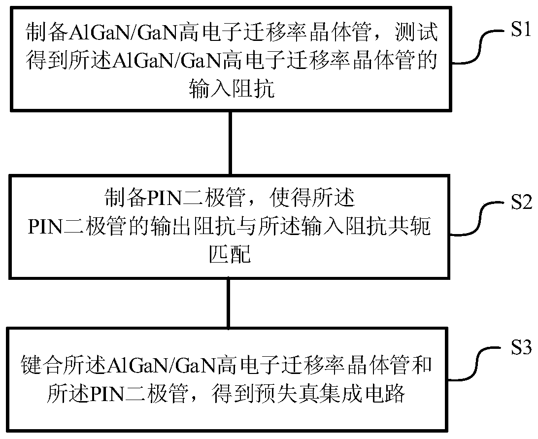
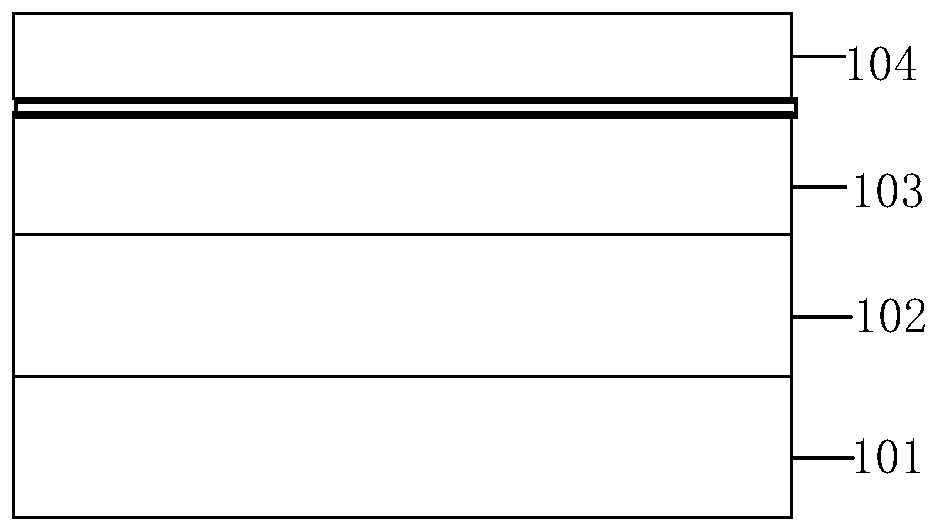
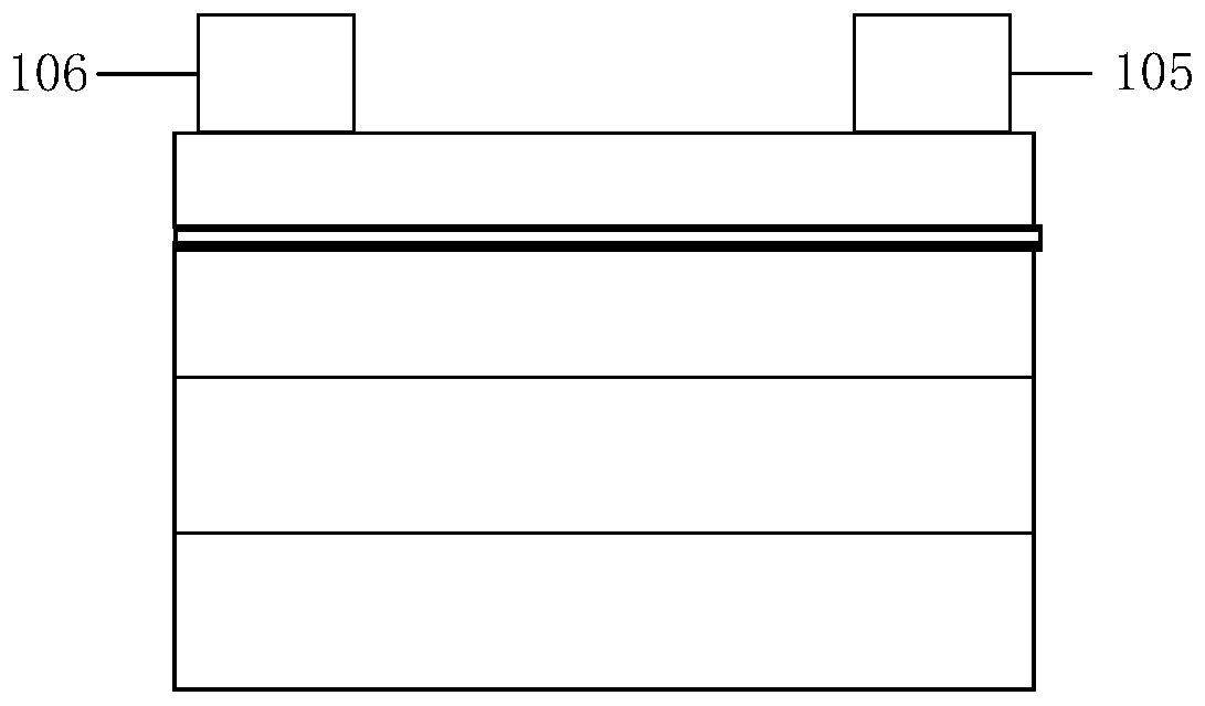
[0058] See figure 1 , figure 1 The flow chart of the manufacturing method of the millimeter-wave predistortion integrated circuit based on the PIN diode provided by the embodiment of the present invention, the AlGaN / GaN high electron mobility transistor includes the first substrate layer 101, the nucleation layer 102, the GaN buffer layer 103 and the AlGaN Fabricated on a sample of the barrier layer 104, see Figure 2a , wherein a two-dimensional electron gas (Two dimensional electrons, 2DEG) exists between the buffer layer 103 and the barrier layer 104 . First, clean the sample. The cleaning steps are as follows: place the sample in acetone for 2 minutes, and then boil it in a positive glue stripping solution heated in a water bath at 60°C for 10 minutes. After cleaning the remaining acetone and ethanol with deionized water, the sample was cleaned with HF solution for 30 seconds, and finally cleaned with deionized water and dried with ultra-pure nitrogen.
[0059] After clea...
Embodiment 2
[0112] See Figure 3a-Figure 3g , Figure 3a-Figure 3g It is a schematic diagram of the manufacturing method of the PIN diode provided by the embodiment of the present invention.
[0113] According to the measured input impedance of the AlGaN / GaN HEMT device, the output impedance of the PIN diode is Z d = r 1 +jxΩ, the junction capacitance of the PIN diode can be calculated from the output impedance. From the junction capacitance, it is known that the size of the PIN diode and the GaN doping concentration affect its size, thereby controlling the output impedance of the PIN diode. Therefore, by controlling the size of the PIN diode and Doping concentration to make PIN diodes.
[0114] PIN diodes are fabricated on a second substrate layer 201 of definite size, see Figure 3a . The specific production steps are as follows:
[0115] S201, epitaxially N+ layer material, I layer material and P+ layer material on the second substrate layer 201, and sequentially form N+ layer 20...
Embodiment 3
[0141] In the embodiment of the present invention, the AlGaN / GaN HEMT and the PIN diode are bonded and assembled through a bonding material to form a predistortion integrated circuit, and the steps are as follows:
[0142] S301. Pretreat the AlGaN / GaN high electron mobility transistor.
[0143] Treat the surface of AlGaN / GaN HEMT devices, through AP3000 treatment liquid and baking, to enhance adhesion;
[0144] S302. Spin-coat a bonding material on the surface of the AlGaN / GaN high electron mobility transistor to form a bonding layer.
[0145] Preferably, the bonding material includes benzocyclobutene (BCB).
[0146] S303, exposing and developing the bonding layer to form a bonding pattern.
[0147] S3031. Set the exposure and development conditions according to the corresponding film thickness, expose the HEMT device spin-coated with BCB material, the photolithographic layout has bonding alignment marks, form a bonding pattern after development, and place the wafer on the h...
PUM
| Property | Measurement | Unit |
|---|---|---|
| thickness | aaaaa | aaaaa |
| thickness | aaaaa | aaaaa |
| thickness | aaaaa | aaaaa |
Abstract
Description
Claims
Application Information


