Low frequency loss gan-based microwave power device and manufacturing method thereof

A technology of microwave power and manufacturing method, applied in the field of microelectronics, can solve problems such as improving and affecting the working performance of devices, and achieve the effects of reducing frequency loss, increasing gate-source spacing, and reducing gate-source parasitic capacitance

Active Publication Date: 2019-10-11
XIDIAN UNIV
View PDF9 Cites 0 Cited by
  • Summary
  • Abstract
  • Description
  • Claims
  • Application Information

AI Technical Summary

Problems solved by technology

However, when the operating frequency is above 30 GHz, the gate-to-drain parasitic capacitance C of the device will be caused by the large dielectric constant of SiN. gd Significantly improved, affecting device performance

Method used


Image

  • Low frequency loss gan-based microwave power device and manufacturing method thereof
  • Low frequency loss gan-based microwave power device and manufacturing method thereof

Examples


Embodiment 1

[0030] Embodiment 1: A low-frequency loss GaN-based microwave power device is manufactured on a SiC substrate with a SiN passivation layer thickness of 200 nm, a BN passivation layer growth thickness of 50 nm, and a passivation layer etching thickness of 60 nm.

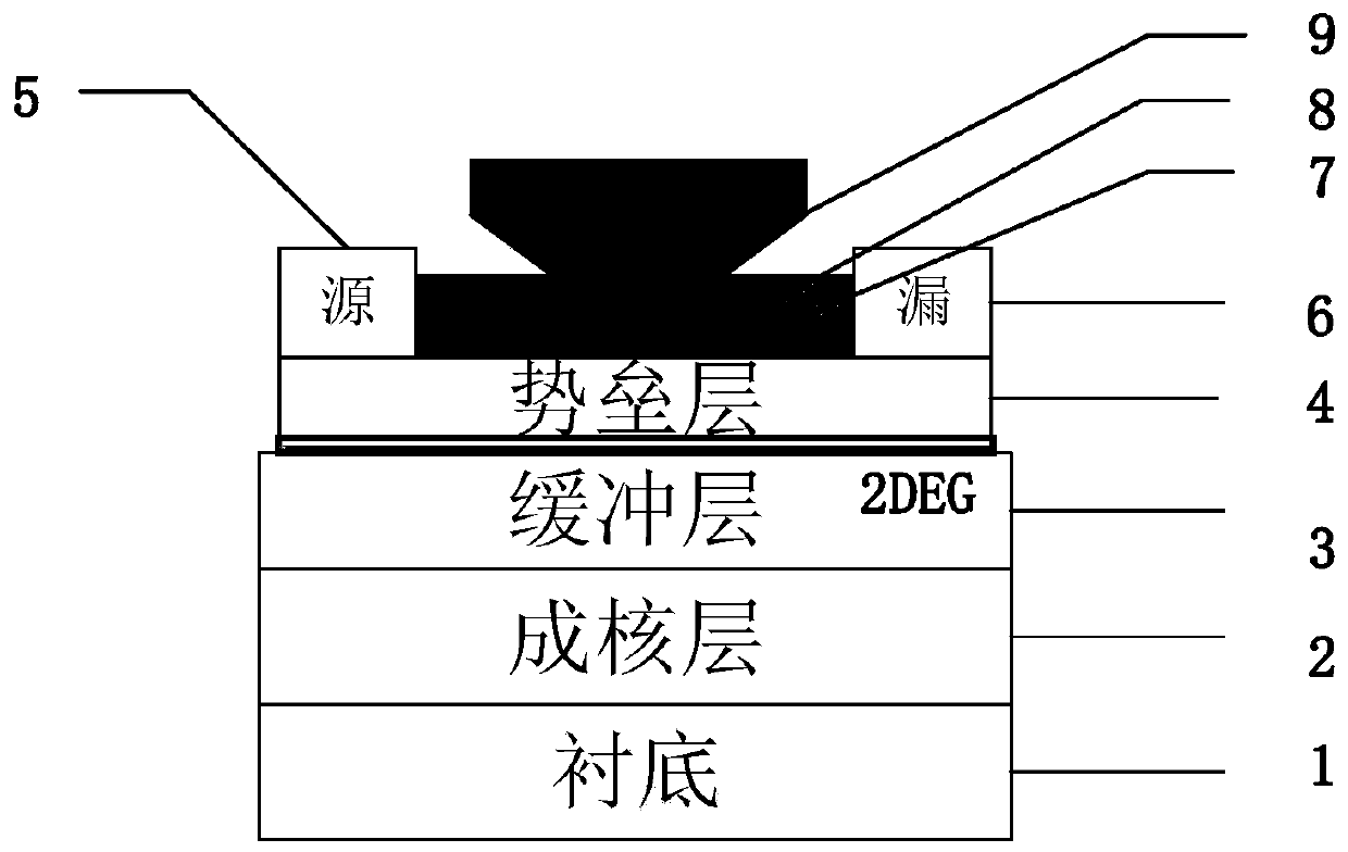
[0031] The device is manufactured on the purchased epitaxial substrate sample which already contains substrate, nucleation layer, buffer layer and potential barrier layer.

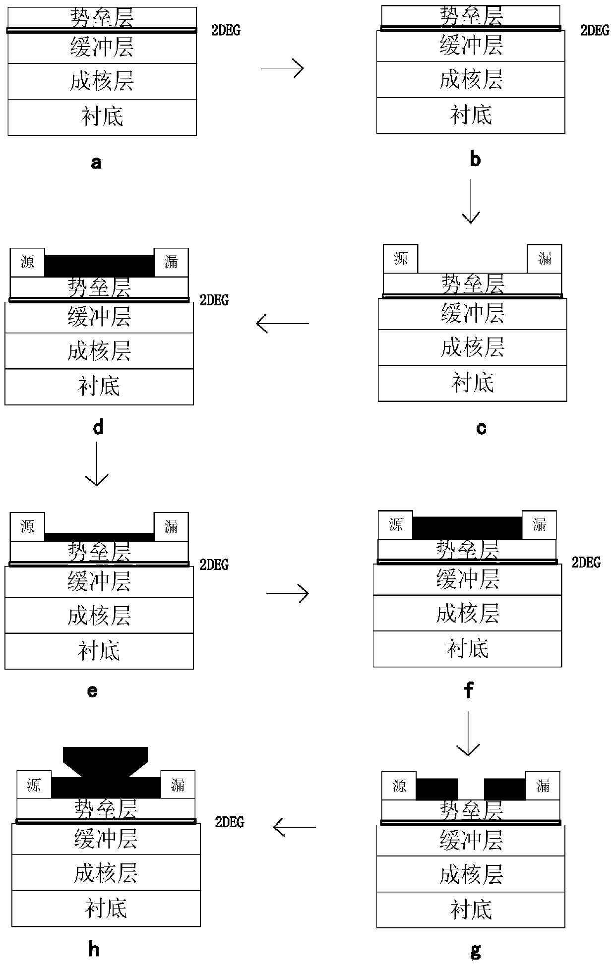
[0032] Step 1, cleaning the epitaxial substrate sample, such as figure 2 (a) shown.

[0033] First place the sample in acetone and sonicate for 2 minutes, then boil it for 10 minutes in a positive glue stripping solution heated in a water bath at 60°C, then place the sample in acetone and ethanol for 3 minutes each, and wash off the residual residue with deionized water. Acetone, ethanol; finally, clean the wafer with HF solution for 30 seconds, then clean it with deionized water and dry it with ultra-pure nitrogen.

[0034] Step 2, use ICP equ...

Embodiment 2

[0106] Embodiment 2, a low-frequency loss GaN-based microwave power device is fabricated on a sapphire substrate with a SiN passivation layer thickness of 100 nm, a BN passivation layer growth thickness of 20 nm, and a passivation layer etching thickness of 30 nm.

[0107] Step 1: Select an epitaxial substrate sample with a substrate, a nucleation layer, a buffer layer, and a barrier layer formed thereon, and clean the substrate.

[0108] The specific implementation of this step is the same as step 1 in the first embodiment.

[0109] Step 2, use ICP equipment to etch the mesa to the barrier layer to realize active area isolation;

[0110] (2.1) Photolithographically isolate regions on the barrier layer:

[0111] The concrete realization of this step is identical with the step 2a) among the embodiment one;

[0112] (2.2) Etching the electrical isolation region on the barrier layer:

[0113] The concrete realization of this step is identical with the step 2b) among the embodi...

Embodiment 3

[0150] Embodiment 3, a low-frequency-loss GaN-based microwave power device is manufactured on a sapphire substrate with a SiN passivation layer thickness of 150 nm, a BN passivation layer growth thickness of 30 nm, and a passivation layer etching thickness of 50 nm.

[0151] In step A, select an epitaxial substrate on which a substrate, a nucleation layer, a buffer layer, and a barrier layer have been formed, and clean the substrate.

[0152] The specific implementation of this step is the same as step 1 in the first embodiment.

[0153] Step B, using ICP equipment to etch the mesa to the barrier layer to realize active area isolation;

[0154] (B1) Photolithographically isolate regions on the barrier layer:

[0155] The concrete realization of this step is identical with the step 2a) among the embodiment one;

[0156] (B2) Etching the electrical isolation region on the barrier layer:

[0157] The concrete realization of this step is identical with the step 2b) among the em...


PUM

PropertyMeasurementUnit
thicknessaaaaaaaaaa
thicknessaaaaaaaaaa
thicknessaaaaaaaaaa

Abstract

The invention discloses a GaN-based microwave power device with low frequency loss. The GaN-based microwave power device comprises a substrate layer (1), a nucleating layer (2), a buffer layer (3) and a barrier layer (4) from bottom to top, wherein a source electrode (5) and a drain electrode (6) are respectively arranged at two ends of the barrier layer, a SiN passivation layer (7) and a BN passivation layer (8) are sequentially arranged on the barrier layer between the source electrode (5) and the drain electrode (6), an opening hole is formed in middle parts of the two passivation layers by etching, and a half-floating grid electrode (9) is led out of the opening hole. A material with a low dielectric constant and low capacitance is employed to form a composite passivation layer with BN and SiN; and compared with a traditional passivation technology, the GaN-based microwave power device has the advantages that the grid-drain parasitic capacitance and the grid-source parasitic capacitance are reduced, the frequency loss of the device is reduced, and the GaN-based microwave power device can be used in communication, satellite navigation, a radar system and a base station system.

Description

technical field [0001] The invention belongs to the technical field of microelectronics, in particular to a GaN-based microwave power device with low frequency loss, which can be used in communication, satellite navigation, radar system and base station system. Background technique [0002] With the improvement of science and technology, the existing first and second generation semiconductor materials can no longer meet the needs of higher frequency and higher power electronic devices, while electronic devices based on nitride semiconductor materials can meet this requirement, greatly The performance of the device has been improved, and the third-generation semiconductor materials represented by GaN have been widely used in the manufacture of microwave and millimeter wave devices. GaN is a new type of wide bandgap compound semiconductor material, which has excellent characteristics that many silicon-based semiconductor materials do not have, such as wide bandgap width, high ...

Claims


Application Information

Patent Timeline
Patent Type & Authority Patents(China)
IPC IPC(8): H01L29/423H01L21/335H01L29/778
Inventor 杨凌芦浩马晓华康慨周小伟宓珉瀚祝杰杰郝跃
Owner XIDIAN UNIV
Why Eureka
Try Eureka