Semiconductor device

A semiconductor and device technology, applied in the field of semiconductor devices, can solve problems such as limiting the application of semiconductor devices, achieve the effect of miniaturizing device integration and improving device integration

Active Publication Date: 2018-01-09
TSINGHUA UNIV +1
View PDF5 Cites 1 Cited by
  • Summary
  • Abstract
  • Description
  • Claims
  • Application Information

AI Technical Summary

Problems solved by technology

[0003] However, limited by the technical level, the heterojunctions in existing semiconductor devices are usually micron structures, which limits the application of semiconductor devices to a certain extent.

Method used


Image

  • Semiconductor device
  • Semiconductor device
  • Semiconductor device

Examples


Embodiment Construction

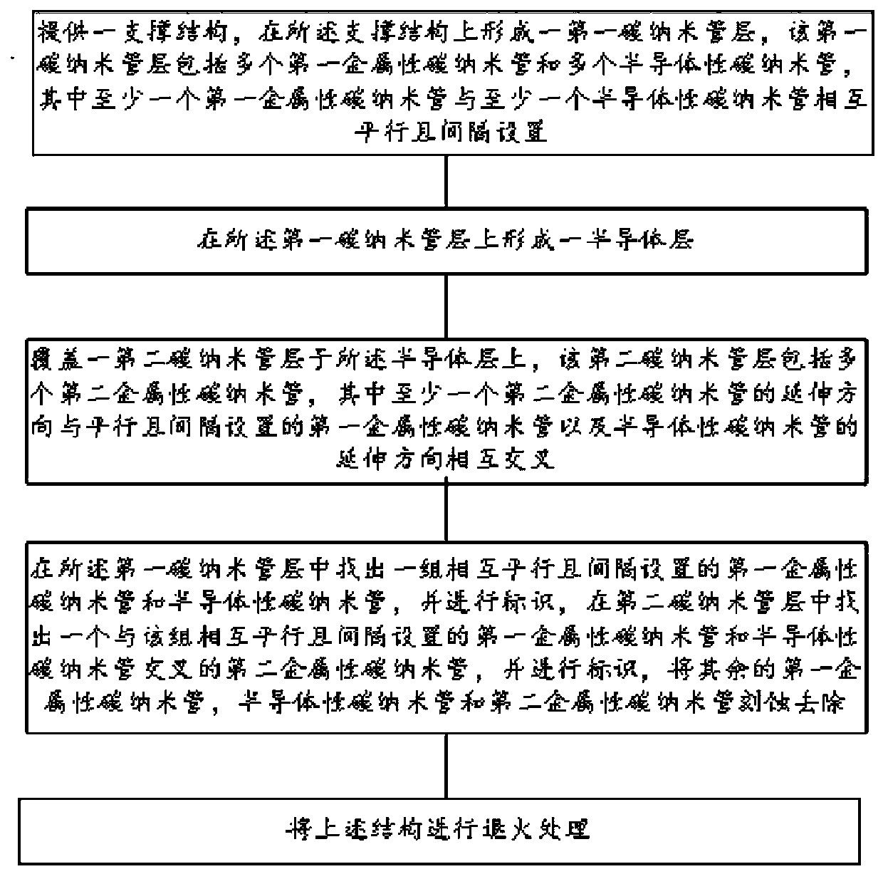
[0015] The nano-heterostructure of the present invention, its preparation method and the semiconductor device using the above-mentioned nano-heterostructure will be further described in detail below with reference to the accompanying drawings.

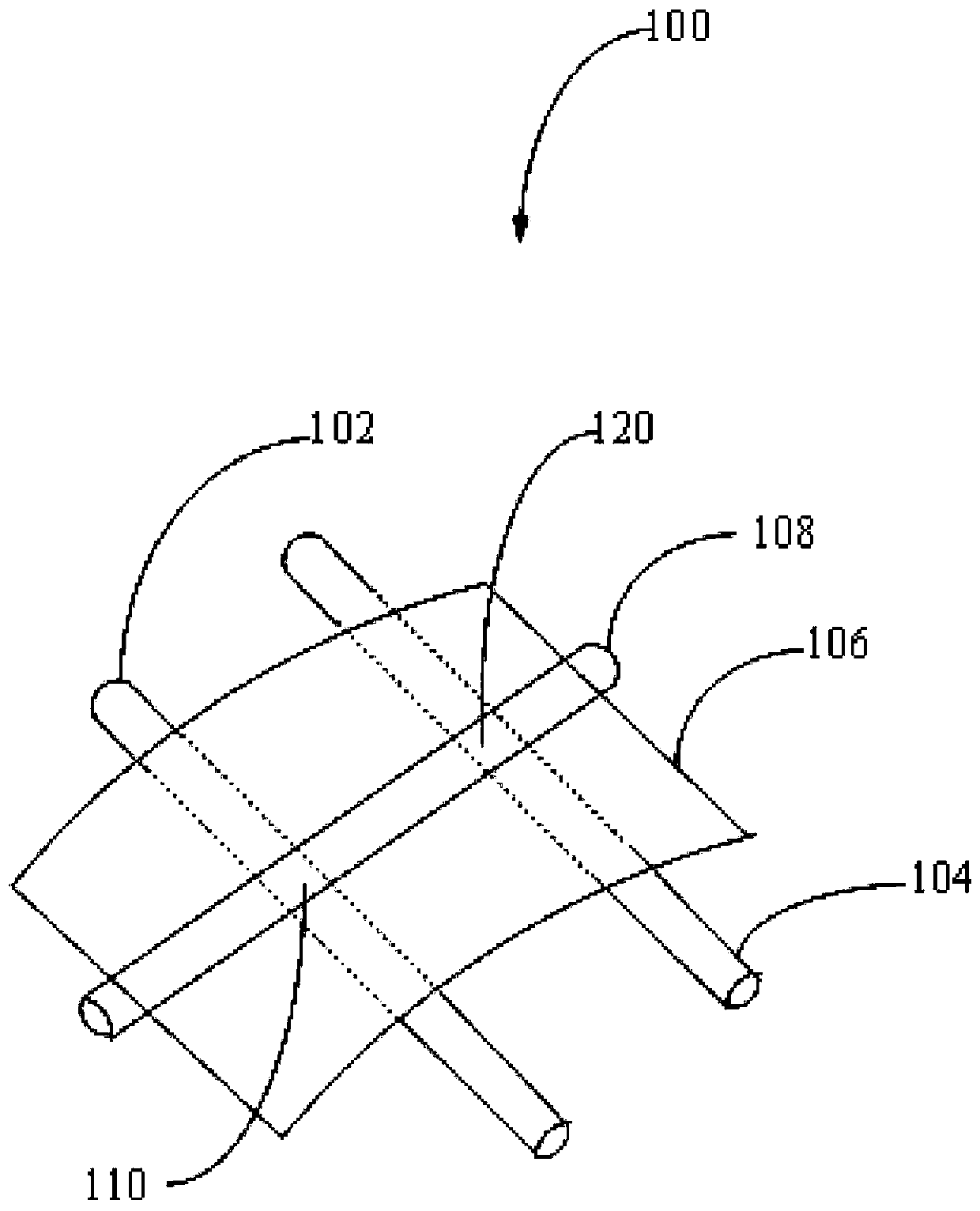
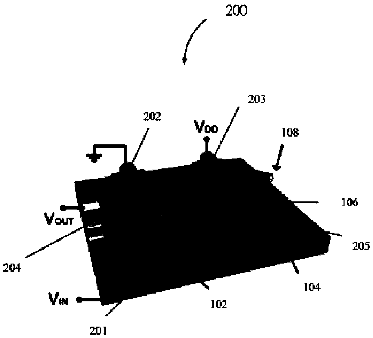
[0016] see figure 1 , the first embodiment of the present invention provides a nano-heterostructure 100 . The nanoheterostructure 100 includes a first metallic carbon nanotube 102 , a semiconducting carbon nanotube 104 , a semiconductor layer 106 and a second metallic carbon nanotube 108 . The semiconductor layer 106 includes a first surface and an opposite second surface, the first metal-type carbon nanotubes 102 and the semiconductor-type carbon nanotubes 104 are arranged on the first surface in parallel and at intervals, and the second metal Type carbon nanotubes 108 are disposed on the second surface. Both the first metal-type carbon nanotubes 102 and the semiconductor-type carbon nanotubes 104 extend toward a first direction, th...


PUM

PropertyMeasurementUnit
diameteraaaaaaaaaa
angleaaaaaaaaaa
thicknessaaaaaaaaaa

Abstract

A semiconductor device comprises a nanometer heterostructure, a first electrode, a second electrode, a third electrode and a fourth electrode; the first electrode is insulated from the second electrode, the third electrode, the fourth electrode and the nanometer heterostructure by an insulation layer; the second electrode, the third electrode, the fourth electrode and the nanometer heterostructureare electrically connected; the nanometer heterostructure comprises a first metallicity carbon nanotube, a semiconductor property carbon nanotube, a semiconductor layer and a second metallicity carbon nanotube; the semiconductor layer comprises a first surface and a second surface in opposite; the first metallicity carbon nanotube and the semiconductor property carbon nanotube are arranged in parallel at an interval on the first surface; the second metallicity carbon nanotube is arranged on the second surface; the first metallicity carbon nanotube and the semiconductor property carbon nanotube extend in the first direction; the second metallicity carbon nanotube extends in the second direction; the second direction and the first direction form an angle, and the formed angle is bigger than0 degree and smaller than or equal to 90 degrees.

Description

technical field [0001] The present invention relates to a semiconductor device. Background technique [0002] A heterojunction is an interface region formed by the contact of two different semiconductor materials. According to the different conductivity types of the two materials, heterojunctions can be divided into homogeneous heterojunctions (P-p junctions or N-n junctions) and heterogeneous heterojunctions (P-n or p-N) junctions. Multilayer heterojunctions are called heterostructures. Usually the conditions for forming heterogeneity are: two semiconductors have similar crystal structure, similar atomic distance and thermal expansion coefficient. Using interfacial alloys, epitaxial growth, vacuum deposition and other techniques, heterojunctions can be fabricated. Heterojunctions often have excellent optoelectronic properties that cannot be achieved by the PN junctions of the two semiconductors, and semiconductor devices made of heterojunctions also have excellent optoele...

Claims


Application Information

Patent Timeline
Patent Type & Authority Applications(China)
IPC IPC(8): H01L27/092B82B3/00B82B1/00
CPCH01L29/66969H01L29/778H01L29/413Y02E10/549H10K19/10H10K85/221H10K10/26H10K10/29H10K30/821H10K30/352
Inventor 张金魏洋姜开利范守善
Owner TSINGHUA UNIV
Why Eureka
Try Eureka