Non-handshake-type JTAG debugging link compatible to AHB protocol and debugging method thereof

A protocol and link technology, applied in the field of integrated circuit design and testing, can solve problems such as consumption and multi-chip resources, and achieve the effect of high application value, strong portability, and stability improvement

Active Publication Date: 2018-01-12
XIAN MICROELECTRONICS TECH INST
View PDF7 Cites 21 Cited by
  • Summary
  • Abstract
  • Description
  • Claims
  • Application Information

AI Technical Summary

Problems solved by technology

However, the patent does not involve specific design details, and the debugging interface is only used in the chip deb...

Method used


Image

  • Non-handshake-type JTAG debugging link compatible to AHB protocol and debugging method thereof
  • Non-handshake-type JTAG debugging link compatible to AHB protocol and debugging method thereof
  • Non-handshake-type JTAG debugging link compatible to AHB protocol and debugging method thereof

Examples


Embodiment

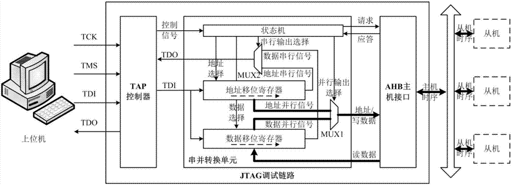
[0093] The SoC compatible with the SPARC V8 structure processor is adopted, and the SoC uses the non-handshaking high-speed JTAG debugging link design structure compatible with the AHB protocol in the present invention, and effectively completes the read-write access of on-chip resources and the infusion of programs. Compared with traditional debugging methods, this debugging structure has higher speed and better stability, and reuses the standard DFT JTAG interface, saving chip pin resources. The invention has high practical value and versatility because it constructs a standard JTAG interface and an on-chip AMBA bus conversion channel.

[0094] Tests have shown that under 180nm process conditions, the traditional RS232 debugging link needs to occupy two additional signal pins, its frequency is 100MHz, its area is 0.372um2, and its maximum communication baud rate is 115200bps; while the compatible AHB in the present invention The non-handshaking high-speed JTAG debugging link...


PUM


Abstract

The invention discloses a non-handshake-type JTAG debugging link compatible to an AHB protocol and a debugging method thereof. The link comprises a deserializing unit which is provided with an external JTAG standard interface on one side and an AHB standard host interface on the other side, and the deserializing unit utilizes a user-defined TAP controller instruction of an IEEE 1149.1 protocol toachieve seamless connection with the AHB protocol through an extension instruction; on the basis of mutual parsing of information, a high-speed serial debugging command sent by an upper computer is mapped onto communication channels of the interior of a chip, an access command is sent to the whole system of the chip to simulate the behaviors of a host, and then the key status information about system running is converted into serial data again and sent back to the upper computer. Compared with traditional debugging approaches, the method has the advantages of being higher in speed and better in stability, since the JTAG interface of standard DFT is repeatedly used, pin resources of the chip are saved, and by establishing a conversion channel between the standard JTAG interface and an on-chip AMBA bus, the method has high practical value and universality.

Description

technical field [0001] The invention belongs to the technical field of integrated circuit design and testing, and in particular relates to a non-handshaking JTAG debugging link compatible with the AHB protocol and a debugging method thereof. Background technique [0002] With the rapid development of microelectronics technology, the integration level of monolithic transistors has increased rapidly. Among them, the SoC design methodology driven by IP multiplexing makes the functional components of a single chip increasingly rich and complex. However, with the integration of many high-speed and complex storage control, communication protocol node control, and digital-analog mixed IP, the problem of full-chip function debugging has become an increasingly serious problem in high-density chip integration design. How to quickly and efficiently trace the fault phenomenon and provide a basis for analyzing the cause of the fault has become an important design task of the debuggable d...

Claims


Application Information

Patent Timeline
IPC IPC(8): G06F13/42
Inventor 娄冕张洵颖杨博崔媛媛肖建青
Owner XIAN MICROELECTRONICS TECH INST
Why Eureka
Try Eureka