Supercharge Your Innovation With Domain-Expert AI Agents!

Half period time delay circuit

A delay circuit, half-cycle technology, applied in the direction of electrical components, pulse processing, pulse technology, etc., can solve the problems of signal transmission distortion, large area and power consumption cost, multiple MOS tubes, etc., and achieve strong resistance to common mode noise interference ability, enhanced resistance, and the effect of saving chip area

Active Publication Date: 2018-01-12
IPGOAL MICROELECTRONICS (SICHUAN) CO LTD
View PDF3 Cites 0 Cited by
  • Summary
  • Abstract
  • Description
  • Claims
  • Application Information

AI Technical Summary

Problems solved by technology

When the value of N is large, the entire circuit needs more MOS transistors, which consumes a large area and power consumption cost
in addition, figure 2 The D flip-flop shown is a single-ended signal input and output, and the single-ended signal has a weak ability to resist external common-mode interference (such as unstable ripple on the power supply), which may easily cause distortion of signal transmission

Method used


Image

  • Half period time delay circuit
  • Half period time delay circuit
  • Half period time delay circuit

Examples


Embodiment Construction

[0021] Embodiments of the present invention will now be described with reference to the drawings, in which like reference numerals represent like elements. As mentioned above, the present invention provides a half-cycle delay circuit. The half-cycle delay circuit of the present invention reduces the number of field effect transistors that need to be used, saves power consumption and the area occupied by chips; at the same time, it enhances the Anti-common mode noise interference capability.

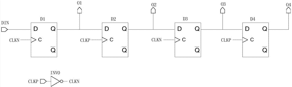
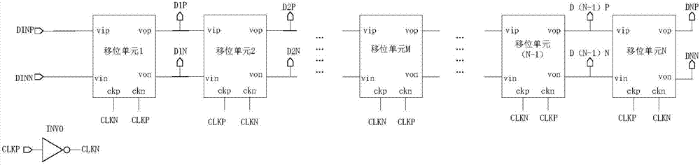
[0022] Please refer to image 3 , image 3 Structural diagram of the half-period delay circuit of the present invention. As shown in the figure, the half-cycle delay circuit of the present invention carries out N half-cycle delays to the input digital signal (DINN, DINP); the half-cycle delay circuit of the present invention includes an inverter INV0 and N shift unit (shift unit 1, 2...N), and N is a natural number greater than 1. Of course, in actual use, the value of N can be flexibl...


PUM


Abstract

The invention discloses a half period time delay circuit. Delay of N half periods is carried out on input digital signals. The half period time delay circuit comprises a phase inverter and N shift units. Each shift unit is equipped with two differential signal input ends and two differential signal output ends. Each shift unit is also equipped with two differential clock input ends. A pair of external differential signals are input into the differential input ends of the first shift unit. The differential output ends of an Nth shift unit output delayed differential signals. The differential output ends and the differential input ends of the other shift units are connected in sequence. An external clock signal is input into the input end of the phase inverter. The external clock signal andthe clock signal output by the phase inverter form a pair of differential clock signals. The differential clock signals are input into the differential clock input ends of the shift units. The N is anatural number greater than 1. According to the half period time delay circuit provided by the invention, the number of field-effect transistors needing to be employed is reduced, the power consumption is reduced, an area occupied by a chip is reduced, and the common-mode noise interference resistance is improved.

Description

technical field [0001] The invention relates to the field of integrated circuits, in particular to a half-period delay circuit for delaying input differential digital signals by N half-periods. Background technique [0002] In some specific integrated circuit applications, such as high-speed data interface circuits, it is usually necessary to delay the digital signal by N / 2 clock cycles, that is, the delay of N half cycles, and the module that realizes the delay of N half cycles is half cycle delay circuit. [0003] At present, the half-cycle delay circuit in the prior art is formed by cascading N D flip-flops, such as figure 1 As shown (taking the case of N=4 as an example), the half-period delay circuit includes four D flip-flops D1, D2, D3, D4. Wherein, the clock input terminal of the odd-numbered D flip-flop is connected to the clock signal CLKN, and the clock input terminal of the even-numbered D flip-flop is connected to the clock signal CLKP (such as figure 1 As sh...

Claims


Application Information

Patent Timeline
Patent Type & Authority Applications(China)
IPC IPC(8): H03K5/134H03K5/00
Inventor 何力
Owner IPGOAL MICROELECTRONICS (SICHUAN) CO LTD
Features
  • R&D
  • Intellectual Property
  • Life Sciences
  • Materials
  • Tech Scout
  • Unparalleled Data Quality
  • Higher Quality Content
  • 60% Fewer Hallucinations
Learn More