Epitaxial filling method for groove

A filling method and trench technology, applied in electrical components, semiconductor/solid-state device manufacturing, circuits, etc., can solve problems such as device failure

Inactive Publication Date: 2018-01-19
SHANGHAI HUAHONG GRACE SEMICON MFG CORP
View PDF3 Cites 3 Cited by
  • Summary
  • Abstract
  • Description
  • Claims
  • Application Information

AI Technical Summary

Problems solved by technology

The void will directly

Method used


Image

  • Epitaxial filling method for groove
  • Epitaxial filling method for groove
  • Epitaxial filling method for groove

Examples


Embodiment Construction

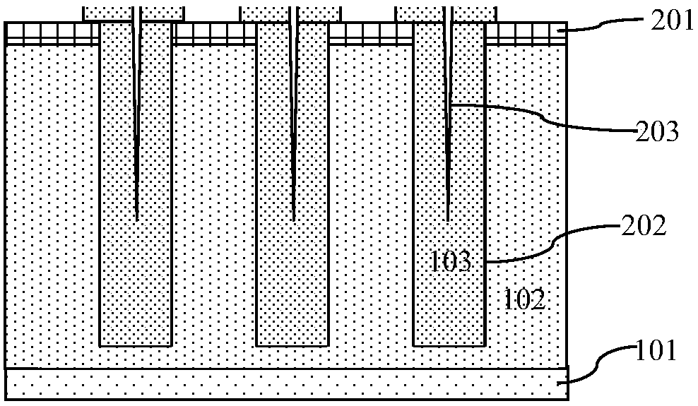
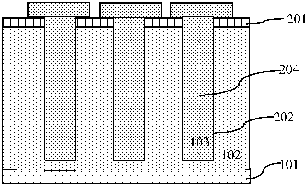
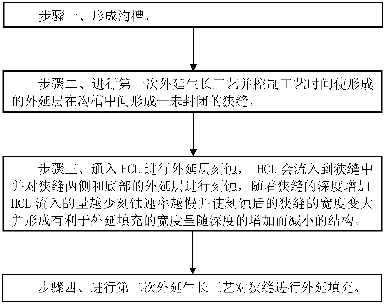
[0026] First introduce the problems that the existing methods have. The method of the embodiment of the present invention has made specific improvements to these technical problems, such as Figure 1A to Figure 1B As shown, it is a schematic diagram of the device structure in each step of the epitaxial filling method of the existing trench; the trench as a superjunction trench is used as an example for illustration, and the existing method includes the following steps:

[0027] Step 1, such as Figure 1A As shown, a semiconductor wafer 101 is provided, and a first conductivity type epitaxial layer 102 is formed on the surface of the semiconductor wafer 101 . Form a hard mask layer 201 on the surface of the epitaxial layer 102 of the first conductivity type, use photolithography to define the formation area of ​​the groove of the super junction, and sequentially apply the hard mask layer in the formation area of ​​the groove 201 and the first conductivity type epitaxial layer ...


PUM


Abstract

The invention discloses an epitaxial filling method for a groove. The method comprises the following steps of (1) forming a groove; (2) carrying out first epitaxial growth process and controlling theprocess time to form an unclosed slot in the middle of the groove through formed epitaxial layers; (3) introducing HCL for epitaxial layer etching, wherein the HCL flows into the slot and etches the epitaxial layers at two sides and the bottom of the slot, the inflow amount of the HCL is reduced and the etching rate is reduced along with a depth increase of the slot, the width of the etched slot is increased and a structure of facilitating reduction of the epitaxial filling width along with the depth increase is formed; and (4) carrying out second epitaxial growth process for epitaxial fillingon the slot. By using the structure of reducing the width of the slot along with the depth increase, a process gas in the second epitaxial growth process smoothly reaches the bottom of the slot, thereby achieving void-free filling. According to the epitaxial filling method, void-free filling can be achieved, a device failure generated by a void can be prevented and the yield of a product can be improved.

Description

technical field [0001] The invention relates to a manufacturing process method of a semiconductor integrated circuit, in particular to an epitaxial filling method of a groove. Background technique [0002] The super junction is composed of alternately arranged P-type thin layers and N-type thin layers formed in a semiconductor wafer (wafer). The existing super junction manufacturing method usually adopts the trench filling process method, and the trench filling method requires First, etch a trench with a certain depth and width on the epitaxial layer on the surface of a semiconductor wafer such as a silicon wafer, such as an N-type doped epitaxial layer, and then fill the etched trench with P Type-doped silicon epitaxy, and requires the filling region to have a complete crystal structure, so that high-performance devices can be fabricated in subsequent processes. [0003] With the development of technology, in the super junction project, on the basis of the second-generatio...

Claims


Application Information

Patent Timeline
IPC IPC(8): H01L21/762
Inventor 伍洲
Owner SHANGHAI HUAHONG GRACE SEMICON MFG CORP
Why Eureka
Try Eureka