A high-resolution display device
A technology for display devices and display areas, applied to static indicators, printed circuits, stacked printed circuit boards, etc., can solve the problems of shrinking display areas, increasing the number of pad terminals, and reducing the brightness of display devices, so as to prevent the increase in resistance big effect
- Summary
- Abstract
- Description
- Claims
- Application Information
AI Technical Summary
Problems solved by technology
Method used
Image
Examples
Embodiment approach
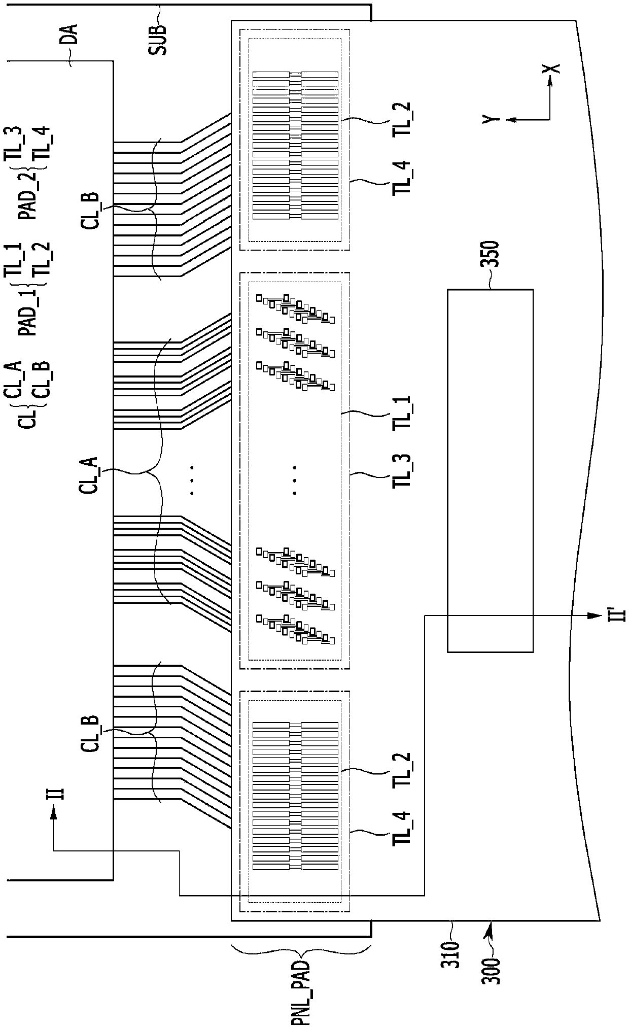
[0089] That is, according to the present exemplary embodiment, the second pad unit PAD_2 of the printed circuit board (PCB) 300 may be formed in a shape corresponding to the first pad unit PAD_1 of the substrate SUB. That is, a plurality of pad terminals arranged in the second pad unit PAD_2 may be arranged in the same or similar pattern as the pad terminals of the first pad unit PAD_1 . The structures of the third terminal region TL_3 and the fourth terminal region TL_4 will be described in further detail below.
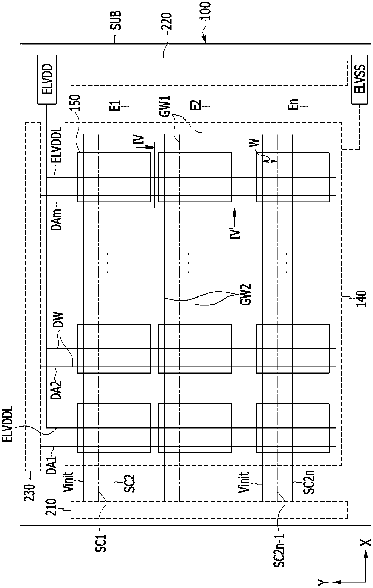
[0090] Next, we will refer to image 3 with Figure 4 The display panel 100 formed in the display area DA is described.
[0091] image 3 is showing figure 1 A schematic diagram of the display area DA, and Figure 4 is along image 3 A sectional view taken along the line IV-IV'.
[0092] According to the present exemplary embodiment, the display panel 100 includes first gate lines GW1 , second gate lines GW2 , data lines DW, a display unit 140 and pixels 150 ...
PUM
 Abstract
Description
Claims
Application Information


