
Circuit board, circuit board manufacturing method, electronic device and assembly method thereof

A technology for electronic equipment and circuit boards, which is applied in printed circuit components, structural connection of printed circuits, printed circuit assembly of electrical components, etc. It can solve problems such as FPC offset production and defects, and achieve accurate alignment work and save energy. Production cost and the effect of improving placement efficiency

Active Publication Date: 2020-06-23
GUANGDONG OPPO MOBILE TELECOMM CORP LTD
View PDF4 Cites 0 Cited by
  • Summary
  • Abstract
  • Description
  • Claims
  • Application Information

AI Technical Summary

Problems solved by technology

At present, FPC is prone to deviation during welding and alignment, resulting in poor production

Method used


Image

  • Circuit board, circuit board manufacturing method, electronic device and assembly method thereof
  • Circuit board, circuit board manufacturing method, electronic device and assembly method thereof
  • Circuit board, circuit board manufacturing method, electronic device and assembly method thereof

Examples


Embodiment 1

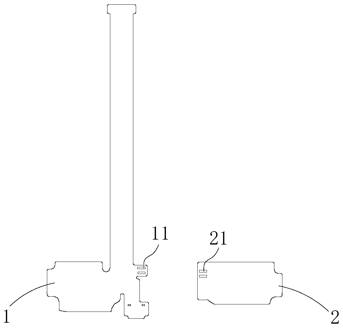
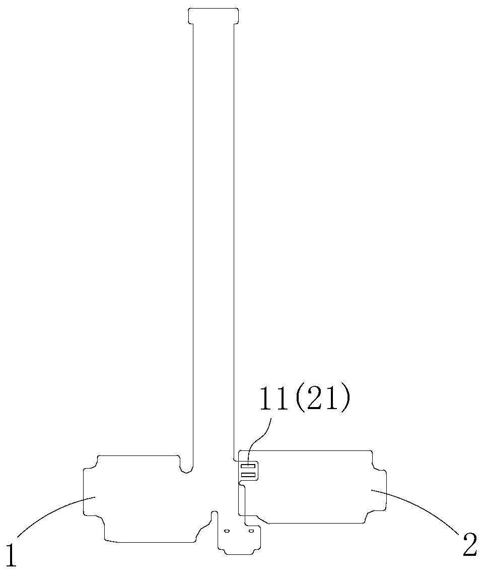
[0045] See figure 1 and figure 2 , the present embodiment provides a circuit board, which includes a main board 1 and a sub-board 2, the main board 1 and the sub-board 2 are provided with splicing parts, and the splicing parts of the two are respectively provided with a splicing pad 11 and a splicing pad 21 , the splicing part of the sub-board 2 and the splicing part of the main board 1 are welded together through the splicing pad 11 and the splicing pad 21 .

[0046] Specifically, the main board 1 is a main circuit board, and the sub-board 2 is a speaker circuit board. In this embodiment, all the main boards 1 and sub-boards 2 are flexible circuit boards; the speaker circuit board and the main circuit board together form a T-shape, wherein the main circuit board is L-shaped. The splicing parts of the main board 1 and sub-board 2 are stacked up and down, the splicing pads 11 and the splicing pads 21 are aligned up and down, and are fixed by solder paste welding.

[0047] T...

Embodiment 2

[0061] This embodiment provides another manufacturing method for the circuit board in Embodiment 1, including the following steps:

[0062] S30. Analyze the shape of the circuit board, define the part protruding from one side of the middle area of ​​the circuit board as sub-board 2, and define the common board formed by the middle area of ​​the circuit board and the part protruding from the other side of the middle area For motherboard 1.

[0063] S31. Divide a circuit board into a main board 1 and sub-boards 2, so that the main board 1 has a larger end and a smaller end, and design splicing pads 11, Stitching pad 12;

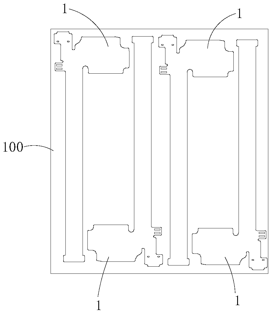
[0064] S32. See Image 6 , at least two main boards 1 are laid out on one imposition 400, and, among two adjacent main boards 1, the larger end of one main board 1 corresponds to the smaller end of the other main board 1, and the sub-boards 2 are arranged on the same On the imposition 400, and the position of the sub-board 2 layout is located in the gap betw...

Embodiment 3

[0070] This embodiment provides another method for making a circuit board, including the following steps:

[0071] S40, see Figure 7a , a circuit board is divided into a main board 1 and two side boards 5, so that the width at both ends of the main board 1 is greater than the middle width, and the area of ​​the two side boards 5 is smaller than the area of ​​the main board 1,

[0072] S41, respectively designing splicing pads at the splicing places of the main board 1 and the side plates 5;

[0073] S42. See Figure 7b , at least two main boards 1 are laid out on one imposition 500, and, among two adjacent main boards 1, the two ends of the main board 1 correspond to the two ends of the other main board 1 respectively, and the side boards 5 are arranged on the same On the imposition 500, and the position of the layout of the side plate 5 is located in the gap between the two main boards 1;

[0074] S43. Paste electronic components on the imposition 500, and then pass throu...


PUM


Abstract

The present invention is applicable to the technical field of electronic equipment, and provides a circuit board, a circuit board manufacturing method, an electronic device and an assembly method thereof. According to the circuit board in the embodiment of the invention, the circuit board comprises a main board and a division board, wherein the main board and the division board are spliced to formthe circuit board. During the designing process for the make-ups of the circuit board, on the condition that the area is kept unchanged, the number of improved make-ups is twice of the original number. In this way, the production cost of the FPC can be reduced by a factor of two simultaneously. At the same time, during the SMD mounting process of the circuit board, a majority of the make-up spaceis fully utilized, so that more electronic components can be pasted on make-up of the same area. Moreover, all electronic components can be unified through a furnace by one time, so that the SMD mounting efficiency is improved. According to electronic device in the embodiment of the invention, a frame is provided with a positioning convex column. During the assembly process, the positioning convex column can penetrate into positioning holes in the main board and the division board which are to be spliced up. As a result, splicing pads on the main board and the division board can be conveniently and accurately aligned with each other.

Description

technical field [0001] The invention belongs to the technical field of electronic equipment, and in particular relates to a circuit board, a method for manufacturing the circuit board, electronic equipment and an assembly method thereof. Background technique [0002] FPC (Flexible Printed Circuit Board, Flexible Printed Circuit) is produced through imposition, and patch needs to go through a whole set of processes. In the main FPC of the existing project, two parts of the circuit board are designed together. For example, the circuit board of the speaker and the circuit board of the antenna part are designed together, so that the lower part takes up more space, and the utilization rate of the FPC is low, because Therefore, the unit price of the waste board part also needs to be calculated during production, so the production cost of FPC is higher. [0003] In addition, the placement is carried out on the imposition, because some areas on the imposition are not designed with ...

Claims


Application Information

Patent Timeline
Patent Type & Authority Patents(China)
IPC IPC(8): H05K1/14H05K3/36
Inventor 范艳辉
Owner GUANGDONG OPPO MOBILE TELECOMM CORP LTD
Learn More