Edge-covered composite antenna module and preparation method thereof
A composite antenna and edge wrapping technology, applied in chemical instruments and methods, lamination, lamination devices, etc., can solve the problems of low production efficiency, long processing cycle and high cost, and achieve efficiency improvement, process cost saving, and material saving Effect
- Summary
- Abstract
- Description
- Claims
- Application Information
AI Technical Summary
Problems solved by technology
Method used
Image
Examples
preparation example Construction
[0035] The preparation method of the edge-wrapped composite antenna module of the present invention comprises the following steps: a. making a composite material layer and affixing the outer double-sided adhesive layer; b. affixing the composite material layer on the cladding layer to unify Do hemming.
[0036] The concrete manufacturing method of described composite material layer is as follows:
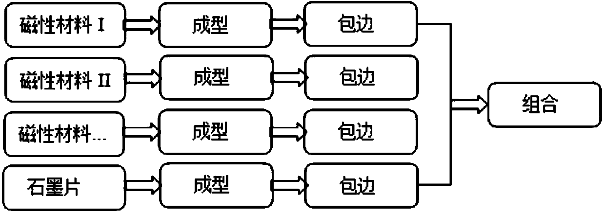
[0037] When the shape of the multi-layer magnetic material layer and the graphite sheet are consistent, the method of pasting and combining first and then forming (cutting out the shape desired by the customer) is adopted (see Figure 7 );
[0038] When the shapes of the multilayer magnetic material layers and the graphite sheets are inconsistent, adopt the method of first forming each and then combining them (see Figure 8 ).
[0039] The present invention is further described by specific examples below:
Embodiment 1
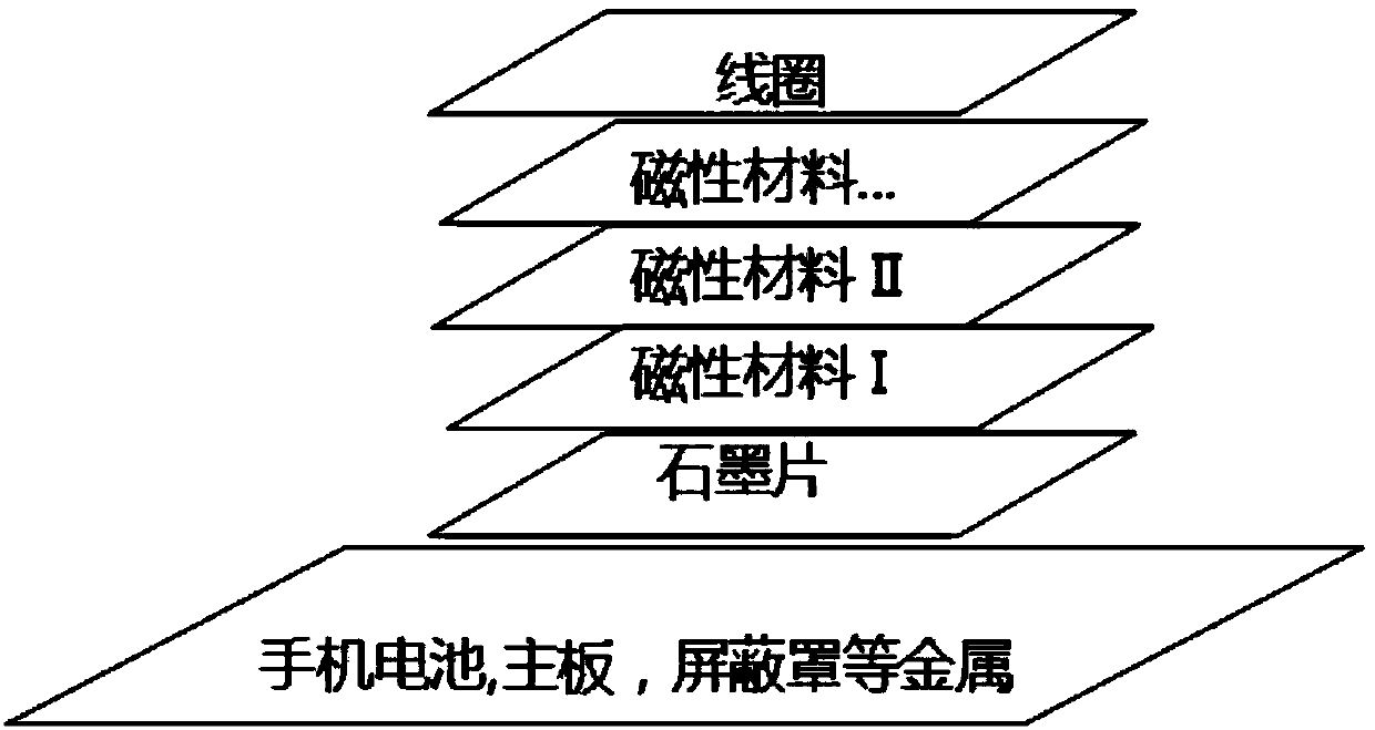
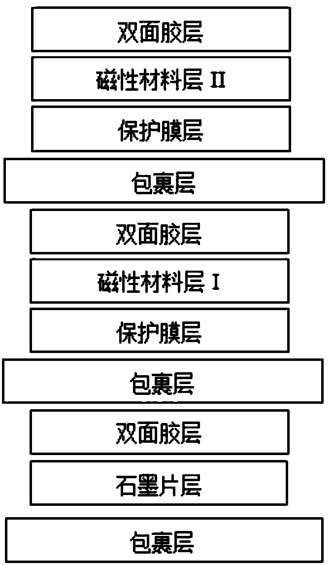
[0041] The antenna module of this embodiment is as Figure 9 As shown, it includes from bottom to top: a wrapping layer, a graphite sheet layer, a first middle double-sided adhesive layer, a wave-absorbing material layer, a second middle double-sided adhesive layer, a nanocrystalline layer, and an outer double-sided adhesive layer.
[0042] Among them, the thickness of the wrapping layer is 10 μm, the thickness of the graphite sheet is 20 μm, the thickness of the first middle double-sided adhesive layer is 5 μm, the thickness of the absorbing material layer is 80 μm, and the thickness of the second middle double-sided adhesive layer is 5 μm, nanometer The thickness of the crystal layer is 50 μm, the thickness of the outer double-sided adhesive layer is 5 μm, and the outer edge of the wrapping layer is 0.8 mm larger than the composite material layer.
[0043] The magnetic material performance list of the present embodiment
[0044]
[0045] The manufacturing method of the a...
Embodiment 2
[0047] The antenna module of this embodiment is as Figure 10 As shown, it includes from bottom to top: wrapping layer, graphite sheet layer, first middle double-sided adhesive layer, absorbing material layer, second middle double-sided adhesive layer, nanocrystalline layer, third middle double-sided adhesive layer, Protective film layer, amorphous layer, outer double-sided adhesive layer.
[0048] Wherein, the thickness of the wrapping layer is 10 μm, the thickness of the graphite sheet is 20 μm, the thickness of the first middle double-sided adhesive layer is 5 μm, the thickness of the wave-absorbing material layer is 75 μm, and the thickness of the second middle double-sided adhesive layer is 5 μm, The thickness of the nanocrystalline layer is 50 μm, the thickness of the third middle double-sided adhesive layer is 5 μm, the thickness of the protective film layer is 10 μm, the thickness of the amorphous layer is 25 μm, the thickness of the outer double-sided adhesive layer i...
PUM
| Property | Measurement | Unit |
|---|---|---|
| thickness | aaaaa | aaaaa |
| thickness | aaaaa | aaaaa |
| thickness | aaaaa | aaaaa |
Abstract
Description
Claims
Application Information


