A kind of epitaxial wafer of light-emitting diode and its preparation method

A technology of light-emitting diodes and epitaxial wafers, which can be applied to semiconductor devices, electrical components, circuits, etc., and can solve the problems of low luminous efficiency of light-emitting diodes

Active Publication Date: 2020-07-07
HC SEMITEK ZHEJIANG CO LTD
View PDF3 Cites 0 Cited by
  • Summary
  • Abstract
  • Description
  • Claims
  • Application Information

AI Technical Summary

Problems solved by technology

[0006] In order to solve the problem of low luminous efficiency of light-emitting diodes in the prior art, an embodiment of the present invention provides an epitaxial wafer of a light-emitting diode and a preparation method thereof

Method used


Image

  • A kind of epitaxial wafer of light-emitting diode and its preparation method
  • A kind of epitaxial wafer of light-emitting diode and its preparation method
  • A kind of epitaxial wafer of light-emitting diode and its preparation method

Examples


Embodiment 1

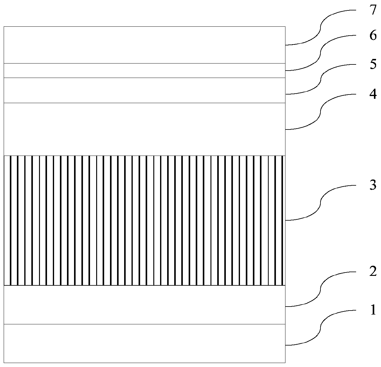
[0030] An embodiment of the present invention provides an epitaxial wafer of a light emitting diode, see figure 1 , the epitaxial wafer includes a substrate 1 and a buffer layer 2, a composite layer 3, an N-type gallium nitride layer 4, a multi-quantum well layer 5, an electron blocking layer 6 and a P-type gallium nitride layer stacked on the substrate 1 in sequence 7.

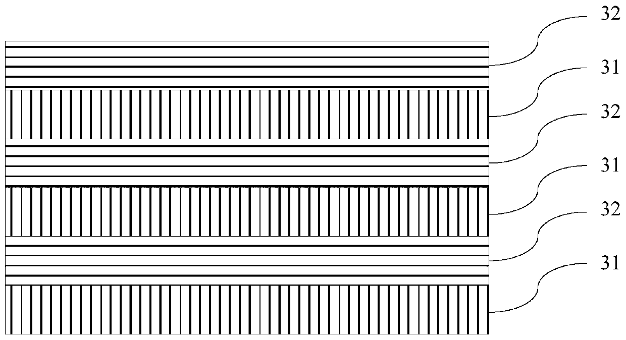
[0031] In this example, see figure 2 The composite layer 3 includes a plurality of gallium nitride layers 31 and a plurality of zinc oxide layers 32, and the plurality of gallium nitride layers 31 and the plurality of zinc oxide layers 32 are alternately stacked.

[0032] In the embodiment of the present invention, a composite layer is provided between the buffer layer and the N-type gallium nitride layer, the composite layer includes multiple gallium nitride layers and multiple zinc oxide layers alternately stacked, and the zinc oxide layer and the gallium nitride layer There is only a 1.9% lattice mismat...

Embodiment 2

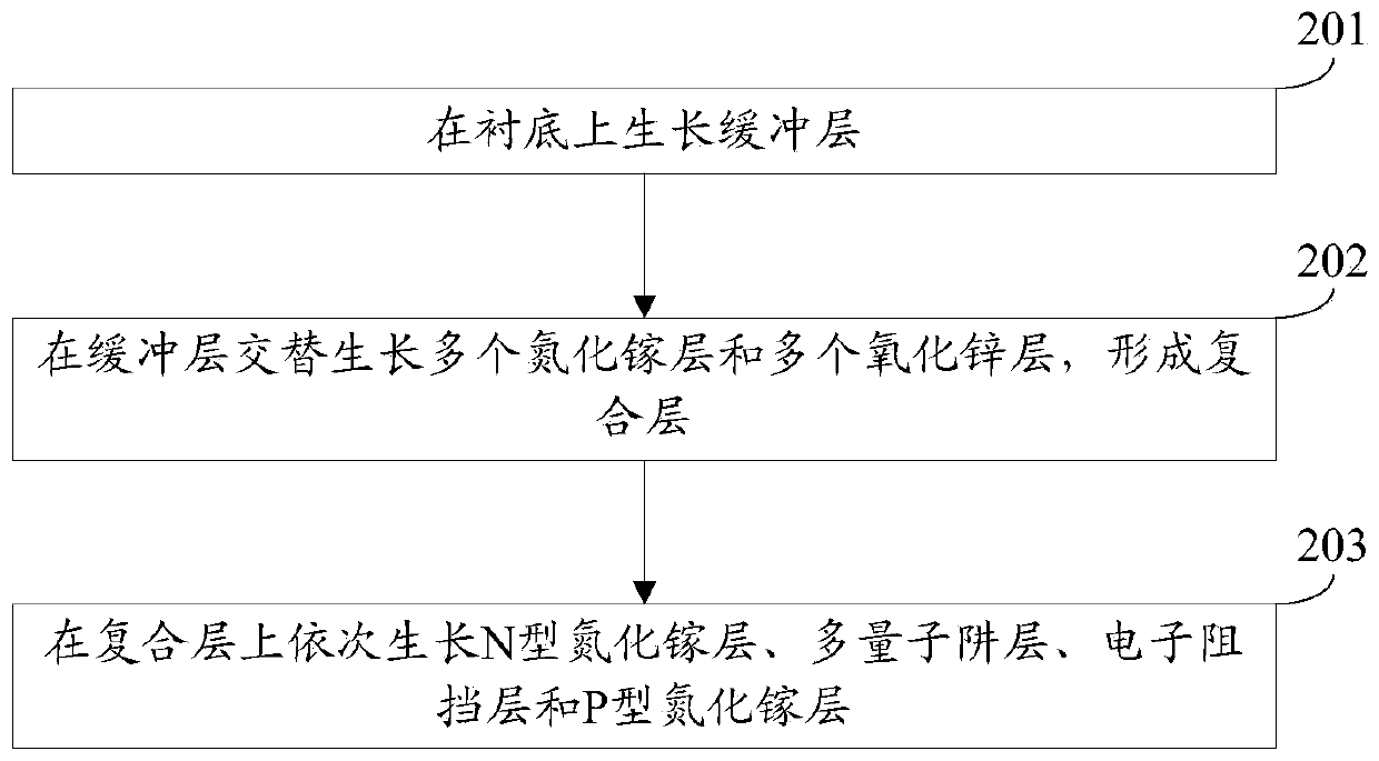
[0048] The embodiment of the present invention provides a method for preparing an epitaxial wafer of a light-emitting diode, which is suitable for preparing the epitaxial wafer provided in Example 1, see image 3 , the preparation method comprises:

[0049] Step 201: growing a buffer layer on a substrate.

[0050] Specifically, this step 201 may include:

[0051] The temperature is controlled at 400° C. to 600° C., the pressure is 400 Torr to 600 Torr, and a gallium nitride layer with a thickness of 15 nm to 35 nm is grown on the sapphire substrate to form a buffer layer.

[0052] Optionally, before step 201, the preparation method may also include:

[0053]Control the temperature to 1100° C., anneal the substrate in a hydrogen atmosphere for 8 minutes, and perform nitriding treatment to clean the substrate.

[0054] Specifically, the substrate can be sapphire with [0001] crystal orientation.

[0055] Optionally, after step 201, the preparation method may further include: ...

Embodiment 3

[0079] The embodiment of the present invention provides a method for preparing an epitaxial wafer of a light-emitting diode, and the preparation method provided in this embodiment is a specific realization of the preparation method provided in Embodiment 2. see Figure 4 , the preparation method comprises:

[0080] Step 301: Control the temperature to 1100° C., anneal the substrate in a hydrogen atmosphere for 8 minutes, and perform nitriding treatment.

[0081] Step 302 : controlling the temperature to 500° C. and the pressure to 500 Torr, growing a gallium nitride layer with a thickness of 25 nm on the sapphire substrate to form a buffer layer.

[0082] Step 303: Control the temperature to 1100° C., the pressure to 500 Torr, and the duration to 7.5 minutes, and perform in-situ annealing treatment on the buffer layer.

[0083] Step 304: controlling the temperature to 1050° C. and the pressure to 300 torr, alternately growing multiple gallium nitride layers and multiple zinc...


PUM

PropertyMeasurementUnit
thicknessaaaaaaaaaa
thicknessaaaaaaaaaa
thicknessaaaaaaaaaa

Abstract

The invention discloses an epitaxial wafer of a light emitting diode and a preparation method thereof, belonging to the technical field of semiconductors. The epitaxial wafer comprises a substrate anda buffer layer, an N-type gallium nitride layer, a multi-quantum well layer, an electron blocking layer and a P-type gallium nitride layer that are sequentially stacked on the substrate, and also comprises a composite layer stacked between the buffer layer and the N-type gallium nitride layer, wherein the composite layer comprises multiple gallium nitride layers and multiple zinc oxide layers, and the multiple gallium nitride layers and the multiple zinc oxide layers are alternately stacked. According to the scheme of the invention, the composite layer is arranged between the buffer layer andthe N-type gallium nitride layer, the composite layer comprises the multiple gallium nitride layers and the multiple zinc oxide layers that are alternately stacked, the dislocation and stress polarization extension caused by lattice mismatch between a sapphire or silicon substrate and gallium nitride can be effectively controlled, the crystal quality of the epitaxial wafer can be improved, a better crystal base for the multi-quantum well layer can be provided, the internal quantum efficiency of the light emitting diode can be improved, and thus the luminous efficiency of the light emitting diode can be improved.

Description

technical field [0001] The invention relates to the technical field of semiconductors, in particular to an epitaxial wafer of a light emitting diode and a preparation method thereof. Background technique [0002] Light Emitting Diode (English: Light Emitting Diode, referred to as: LED) is a semiconductor light emitting device made by using the principle of semiconductor PN junction electroluminescence. The epitaxial wafer is the primary product in the process of manufacturing light-emitting diodes. [0003] The existing epitaxial wafer includes a substrate and a buffer layer, an undoped gallium nitride layer, an n-type gallium nitride layer, a multi-quantum well layer, an electron blocking layer and a p-type gallium nitride layer stacked sequentially on the substrate. Wherein, the multi-quantum well layer includes multiple quantum wells and multiple quantum barriers, the multiple quantum wells and multiple quantum barriers are alternately stacked, the quantum wells are InGa...

Claims


Application Information

Patent Timeline
Patent Type & Authority Patents(China)
IPC IPC(8): H01L33/12H01L33/00
CPCH01L33/007H01L33/12
Inventor 郭炳磊葛永晖魏晓骏吕蒙普胡加辉李鹏
Owner HC SEMITEK ZHEJIANG CO LTD
Why Eureka
Try Eureka