Wire arch detecting method and device in photovoltaic silicon wafer cutting process

A technology for silicon wafer cutting and process detection, which is applied to fine working devices, working accessories, stone processing equipment, etc., can solve the problems of inconvenient operation and insufficient precision, and achieve the effect of accurate results, continuous observation, and reduced detection difficulty.

Pending Publication Date: 2018-02-09
杨凌美畅新材料股份有限公司
View PDF0 Cites 3 Cited by
  • Summary
  • Abstract
  • Description
  • Claims
  • Application Information

AI Technical Summary

Problems solved by technology

[0004] In order to effectively solve the problems of insufficient precision and inconvenient operation existing in the prior art...

Method used


Image

  • Wire arch detecting method and device in photovoltaic silicon wafer cutting process
  • Wire arch detecting method and device in photovoltaic silicon wafer cutting process
  • Wire arch detecting method and device in photovoltaic silicon wafer cutting process

Examples


Embodiment Construction

[0033] The present invention will be described in further detail below in conjunction with the accompanying drawings and embodiments.

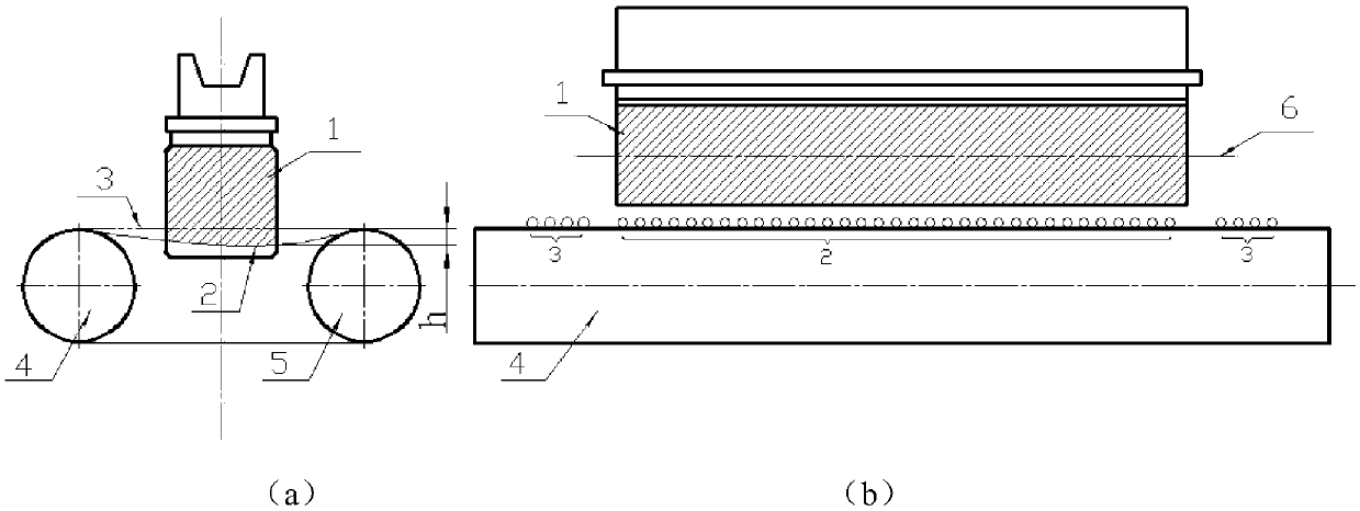
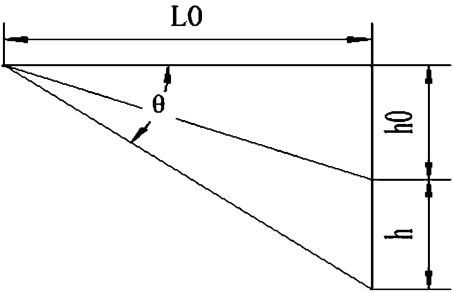
[0034] Such as figure 1 As shown, the essence of line bow measurement is to measure a longitudinal height h.

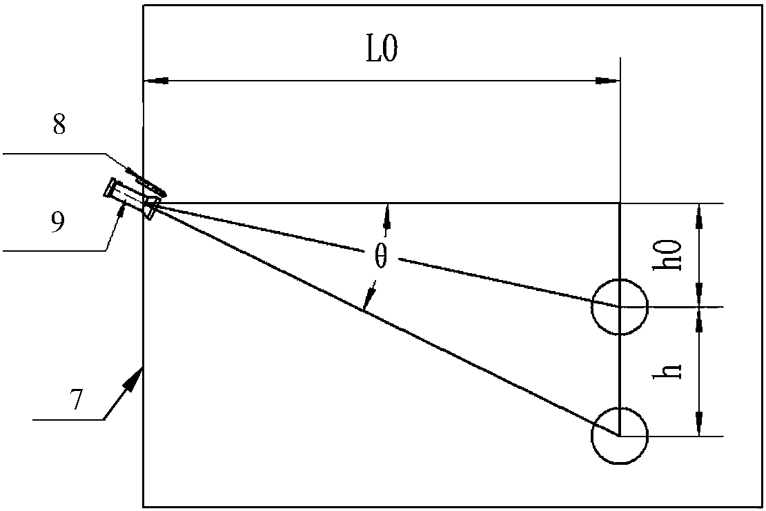
[0035] Such as image 3 As shown, in this embodiment, an independent detection device is set on the cutting chamber wall 7 of the multi-wire cutting machine, that is, a telescopic lens 8 with a transparent scale outside, and a cross mark in the center of the lens. There is a protective cover in front of the lens, open the protective cover before measurement.

[0036] Small-sized lighting fixture 9 and switch are installed in front of the camera lens to provide illumination for observation; the lamp has a protective cover, and the protective cover is opened when the switch is turned on.

[0037] The telephoto lens and lighting fixtures are removable and washable.

[0038] The detection process is as Figure 5 Shown:

[0039] Firs...


PUM


Abstract

The invention proposes a method and device for detecting wire bows during the cutting process of photovoltaic silicon wafers, which can effectively solve the problems of insufficient precision and inconvenient operation existing in the prior art. The device for detecting the wire bow is to fix a telescopic lens with a transparent scale outside the photovoltaic silicon wafer cutting work area, and there is a cross mark in the center of the lens; set the viewing angle of the telescopic lens to observe the wire bow as θ, and measure the distance from the telescopic lens to the cutting wire net The horizontal distance L0 to the junction point of the silicon rod and the height h0 relative to the cutting line network are calculated according to the corresponding relationship between θ and h embodied by h=L0tanθ‑h0 and the vertical height value is marked on the transparent scale, which is used for direct observation. The value h of the wire bow. The detection result of the present invention is accurate (the precision is 1mm); during the detection, it is not necessary to repeatedly open and close the cutting chamber during the cutting process; at the same time, continuous observation is realized, which greatly reduces the detection difficulty of technicians.

Description

technical field [0001] The invention relates to a method and a device for detecting wire bows in the cutting process of hard and brittle materials. Background technique [0002] Photovoltaic silicon wafers are usually manufactured by multi-wire cutting of silicon rods, and the size of the wire bow in the cutting process is a very critical parameter. At present, it is generally approximated by visual observation of the cutting process, and then the stability of the cutting process, the cutting force of the cutting wire (electroplated diamond wire), and the matching degree of the cutting process are evaluated, judged, and adjusted. The so-called wire bow refers to the longitudinal distance between the intersection point of the wire mesh and the silicon rod from the original position. [0003] The main disadvantages of the existing wire bow detection are: visual inspection (long distance, estimated, inaccurate; different observers have large differences); need to open and clos...

Claims


Application Information

Patent Timeline
IPC IPC(8): B28D5/04B28D7/00
CPCB28D5/0058B28D5/045
Inventor 曲东升郭亮王新平曹民博
Owner 杨凌美畅新材料股份有限公司
Why Eureka
Try Eureka