Supercharge Your Innovation With Domain-Expert AI Agents!

ESD (Electro-Static discharge) protection device and circuit protection method

An ESD protection and electrostatic discharge technology, applied in the direction of electric solid devices, circuits, electrical components, etc., can solve the problems of poor heat dissipation, device performance degradation, etc., to achieve the effect of protecting internal circuits, reducing the possibility, and easy heat dissipation

Active Publication Date: 2018-02-09
SEMICON MFG INT (BEIJING) CORP +1
View PDF10 Cites 4 Cited by
  • Summary
  • Abstract
  • Description
  • Claims
  • Application Information

AI Technical Summary

Problems solved by technology

For fin-type gate-controlled diodes, which have relatively narrow fins (Fin), when they work as ESD protection devices, they are prone to poor heat dissipation and serious self-heating problems, which may cause device performance reduce

Method used


Image

  • ESD (Electro-Static discharge) protection device and circuit protection method
  • ESD (Electro-Static discharge) protection device and circuit protection method
  • ESD (Electro-Static discharge) protection device and circuit protection method

Examples


Embodiment Construction

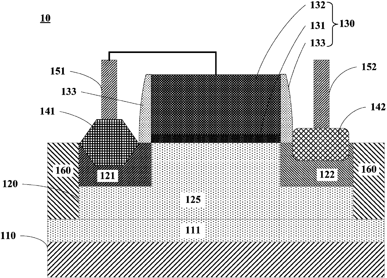
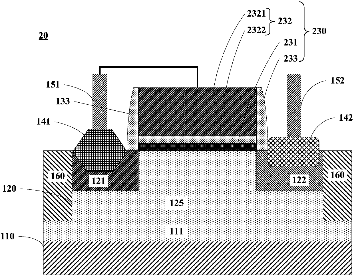
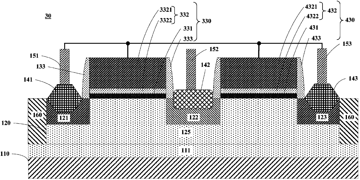
[0041] Various exemplary embodiments of the present invention will now be described in detail with reference to the accompanying drawings. It should be noted that the relative arrangements of components and steps, numerical expressions and numerical values ​​set forth in these embodiments do not limit the scope of the present invention unless specifically stated otherwise.

[0042] At the same time, it should be understood that, for the convenience of description, the sizes of the various parts shown in the drawings are not drawn according to the actual proportional relationship.

[0043] The following description of at least one exemplary embodiment is merely illustrative in nature and in no way taken as limiting the invention, its application or uses.

[0044] Techniques, methods and devices known to those of ordinary skill in the relevant art may not be discussed in detail, but where appropriate, such techniques, methods and devices should be considered part of the Authorized...


PUM


Abstract

The invention discloses an ESD (Electro-Static discharge) protection device and a circuit protection method, which relate to the technical field of semiconductors. The ESD protection device comprisesa semiconductor substrate, a semiconductor fin located on the semiconductor substrate and a gate structure located on the semiconductor fin, wherein the semiconductor fin comprises a first area, a first doping area and a second doping area, and the first doping area and the second doping area are adjacently connected with the first area and are mutually spaced; and the gate structure and the firstdoping area are electrically connected to the same potential. The phenomenon that the gate structure and the first doping area are electrically connected to the same potential is realized. Further, the possibility that the performance of the ESD protection device falls can be reduced.

Description

technical field [0001] The present invention relates to the technical field of semiconductors, in particular to an electrostatic discharge (Electro-Static discharge, ESD for short) protection device and a method for protecting a circuit. Background technique [0002] As the size of MOSFET (Metal Oxide Semiconductor Field Effect Transistor, Metal Oxide Semiconductor Field Effect Transistor) devices decreases gradually, the short channel effect becomes a key issue. The FINFET (FinField Effect Transistor, Fin Field Effect Transistor) device exhibits relatively good gate control ability on the channel charge, so that the size of the CMOS device can be further reduced. [0003] In the prior art, gate-controlled diodes can be applied to ESD protection devices. At present, FINFET technology is applied to the manufacturing process of gate-controlled diodes to manufacture fin-type gate-controlled diodes. For fin-type gate-controlled diodes, which have relatively narrow fins (Fin), ...

Claims


Application Information

Patent Timeline
Patent Type & Authority Applications(China)
IPC IPC(8): H01L23/60H01L29/06H01L29/78
CPCH01L23/60H01L29/06H01L29/78H01L27/0255H01L27/0266H01L29/0847H01L29/42312H01L29/4966H01L29/66356H01L29/7851H01L29/861H01L21/76895H01L23/535H01L29/1095H01L29/42372H01L29/66795
Inventor 周飞
Owner SEMICON MFG INT (BEIJING) CORP
Features
  • R&D
  • Intellectual Property
  • Life Sciences
  • Materials
  • Tech Scout
  • Unparalleled Data Quality
  • Higher Quality Content
  • 60% Fewer Hallucinations
Learn More