Removal method of PCB electroplating lead

A technology of electroplating lead wires and ink plating, which is applied in the fields of electrical components, printed circuits, and printed circuit manufacturing. It can solve problems such as short circuit of electroplating lead wires, excessively long residual wires, and low precision, so as to avoid coverage failure, strong promotion significance, and Easy to remove the effect of the film

Active Publication Date: 2018-02-16
东莞康源电子有限公司
View PDF4 Cites 12 Cited by
  • Summary
  • Abstract
  • Description
  • Claims
  • Application Information

AI Technical Summary

Problems solved by technology

The traditional method of removing the electroplating lead is to remove it by machining, but the precision of the machining removal method is low, and there is a problem that the electroplating lead is not removed cleanly and the lead remains too long or the copper is exposed due to excessive removal. The above problems will lead to gold The electrical parameters of the finger change, and even a short circuit may be caused by the residual plating lead during the plugging and unplugging process

Method used


Image

  • Removal method of PCB electroplating lead

Examples


Embodiment Construction

[0017] In order to make the purpose, technical solution and advantages of the invention clearer, the invention will be further described in detail below in conjunction with the accompanying drawings and embodiments.

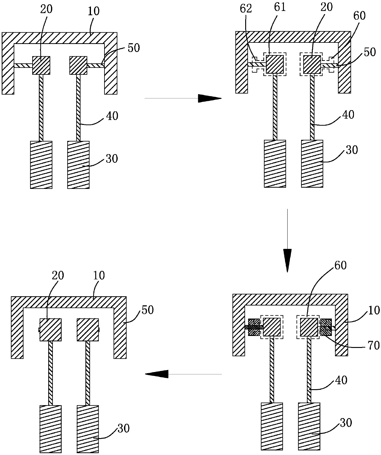
[0018] like figure 1 Shown, the invention provides a kind of removal method of PCB electroplating lead, for removing unnecessary electroplating lead on PCB, the present invention comprises the following steps:

[0019] Step (1), providing a PCB, the PCB is provided with a copper layer 10, a pad 20, a gold finger 30, an impedance line 40, and an electroplating lead 50, and the gold finger 30 is electrically connected to the solder joint through the impedance line 40. On the pad 20 , the pad 20 is connected to the copper layer 10 through the electroplating lead 50 , and the gold finger 30 is plated with gold through the electroplating lead 50 . In addition, a solder resist protection layer (not shown) is provided on the outer sides of the electroplating leads 50 a...


PUM


Abstract

A removal method of a PCB electroplating lead is used for removing an excess electroplating lead on a PCB and comprises a step (1) of providing a PCB on which a copper layer, a pad, a gold finger, animpedance line and an electroplating lead are arranged, wherein the electroplating lead and the pad are both provided with a solder mask protection layer on the outer sides; a step (2) of opening a window in the solder mask protection layer; a step (3) of selecting plating ink; a step (4) of performing pad surface treatment; a step (5) of removing a film; and a step (6) of etching to remove the lead. The beneficial effects of the invention are that the un-removed lead at one end of the pad in the subsequent procedure is made shorter and electrical parameters of the gold finger are more stableby providing the convex window; and the shortcoming of failing to cover the sidewall of the lead can be avoided and the film removal is facilitated by covering the lead with the selected plating ink;the residue of the lead can be reduced by using the etching method to remove the lead; and the removal method is highly practical and has a great significance in popularization.

Description

technical field [0001] The invention relates to the technical field of printed circuit boards, in particular to a method for removing PCB electroplating leads. Background technique [0002] A printed circuit board (Printed Circuit Board, PCB) is the basis of electronic products and is widely used in various electronic devices. At present, some PCBs need to be equipped with gold fingers due to the needs of the connection interface. In the process of making gold fingers, it is necessary to etch out the graphics and gold-plated wires in the board through external drawing and external etching, and then use solder resist ink to cover the non-gold-plated area. , gold-plated by electroplating leads, and finally trimmed the shape. [0003] The electroplating lead is only a process auxiliary line, which is not retained in the final product. After the electroplating is completed, the electroplating lead needs to be removed. The traditional method of removing the electroplating lead ...

Claims


Application Information

Patent Timeline
Patent Type & Authority Applications(China)
IPC IPC(8): H05K3/18
CPCH05K3/18H05K2203/175
Inventor 崔红兵章剑波杜在涯
Owner 东莞康源电子有限公司
Why Eureka
Try Eureka