Integrated ashing and implant annealing method using ozone

a technology of ion implantation and annealing method, which is applied in the field of semiconductor manufacturing methods, can solve the problems of low reactive gas available to the removal process, contaminating the substrate of the chemical bath that is needed to remove the resist, and affecting the effect of ion implantation annealing, so as to achieve the effect of reducing or eliminating the annealing process, reducing or eliminating the vacuum force, and reducing the amount of resis

Inactive Publication Date: 2005-04-21
WAFERMASTERS
View PDF5 Cites 55 Cited by
  • Summary
  • Abstract
  • Description
  • Claims
  • Application Information

AI Technical Summary

Benefits of technology

[0021] Other embodiments include “pulling” exhaust gases from the processing chamber and heating the exhaust gases as the exhaust gases exit the chamber. This can be accomplished with a long exhaust tube coupled to an exhaust port of the chamber, where heaters arranged along the length of the tube. A second exhaust tube, which in one embodiment is perpendicular to the long exhaust tube, can be a venturi that pulls the exhaust gases from the processing chamber, through the long exhaust tube and second exhaust tube. A gas/compressor may be coupled to one end of the second exhaust tube to generate sufficient vacuum force for the venturi. Heating the exhaust gases as they leave the processing chamber prevents condensation from accumulating along the exhaust tube, which may

Problems solved by technology

However, in wet ashing methods the chemical bath that is needed to remove the resist can also contaminate the substrate.
Thus, the amount of reactive gas available to the removal process is low.
Unfortunately, substrate damage can occur as the substrate is exposed to the plasma due to the ion bombardment.
In addition, dry ashing methods usually leave residue on the wafer surface even after the ashing processes are complete.
As a result, the photo

Method used


Image

  • Integrated ashing and implant annealing method using ozone
  • Integrated ashing and implant annealing method using ozone
  • Integrated ashing and implant annealing method using ozone

Examples


Embodiment Construction

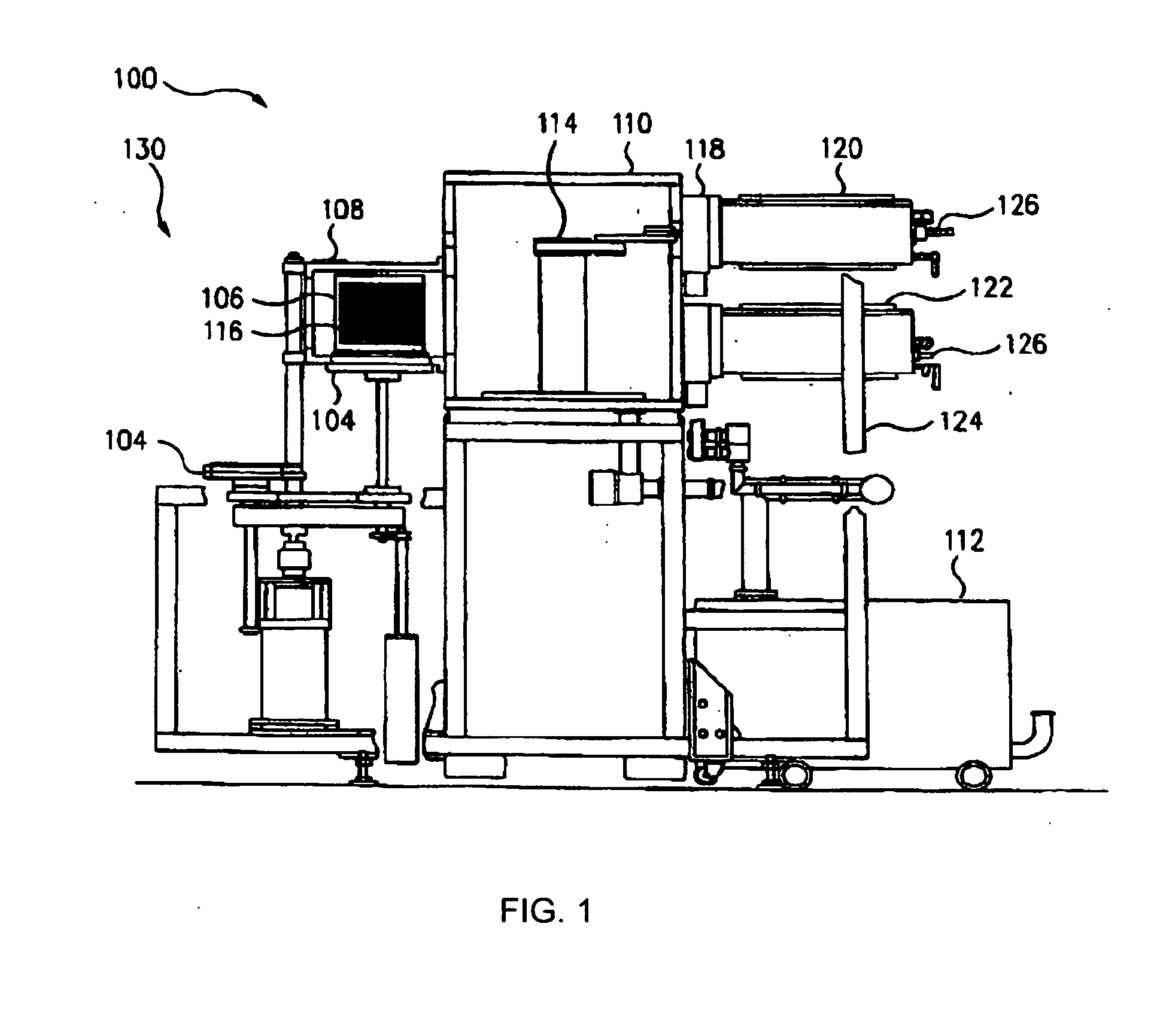
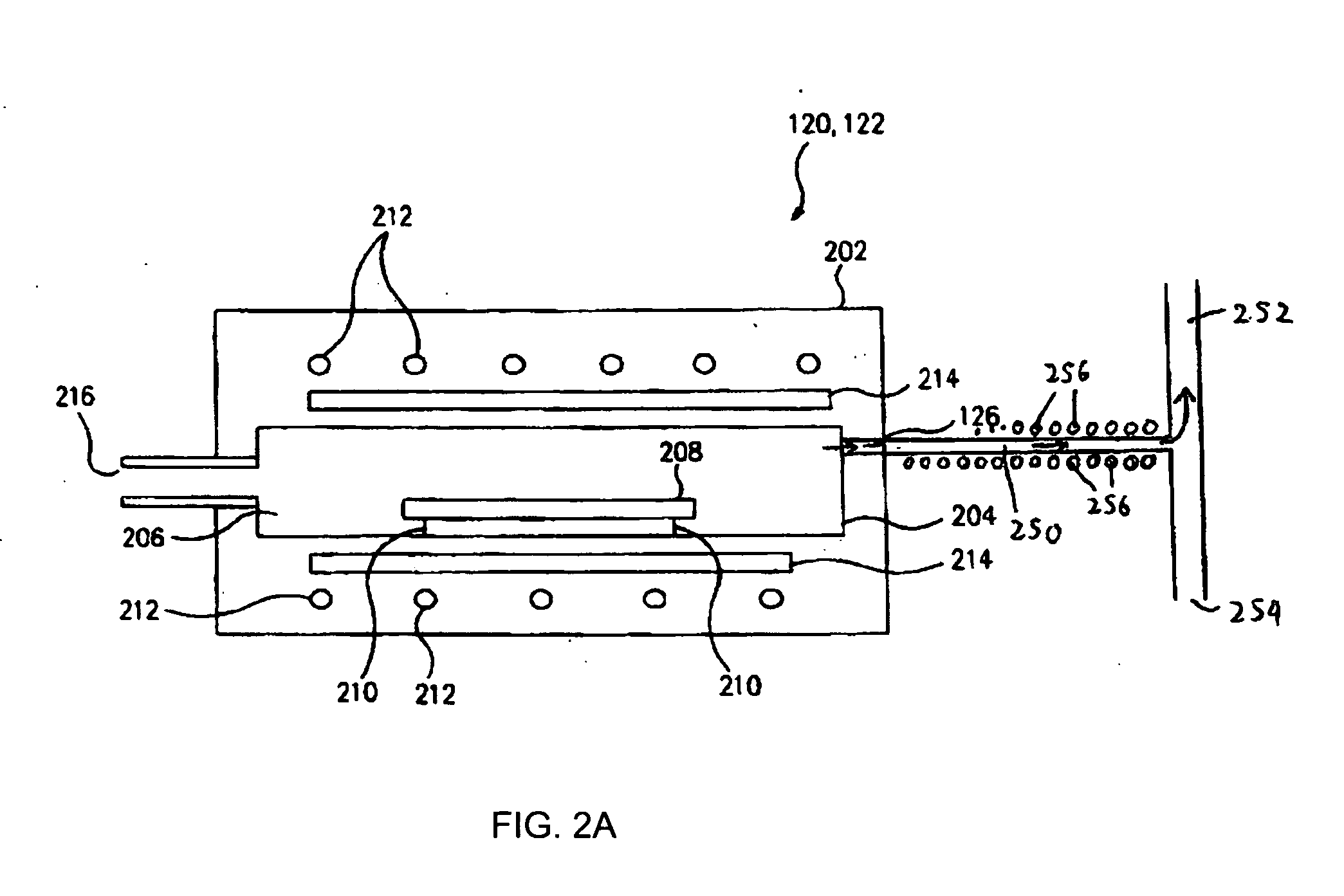
[0031]FIG. 1 is a schematic illustration of a side view of one embodiment of a semiconductor wafer processing system 100 that establishes a representative environment of the present invention. Processing system 100 includes a loading station 130 which has multiple platforms 104 for supporting and moving a wafer cassette 106 up and into a loadlock 108. Wafer cassette 106 may be a removable cassette which is loaded into a platform 104, either manually or with automated guided vehicles (AGV). Wafer cassette 106 may also be a fixed cassette, in which case wafers are loaded onto cassette 106 using conventional atmospheric robots or loaders (not shown). Once wafer cassette 106 is inside loadlock 108, loadlock 108 and transfer chamber 110 are maintained at atmospheric pressure or else are pumped down to vacuum pressure using a pump 112. A robot 114 within transfer chamber 110 rotates toward loadlock 108 and picks up a wafer 116 from cassette 106. A reactor or thermal processing chamber 120...


PUM


Abstract

After ion implantation, thermal ashing is performed using ozone at a pressure of between about 0.01 to about 1000 Torr at below 1000° C. to remove the resist. Since the process includes a substantial amount of ozone, the resist can be completely oxidized, thus leaving no residue or other contaminates to remain on the substrate. Using ozone allows fast resist removal with minimal residue at low temperatures.

Description

CROSS REFERENCE TO RELATED APPLICATIONS [0001] This application is a continuation-in-part of U.S. appl. Ser. No. 10 / 690,315, filed Oct. 20, 2003.BACKGROUND [0002] 1. Field of Invention [0003] This invention generally relates to semiconductor manufacturing methods and, more particularly, to a method for removing organic films and materials used during semiconductor wafer fabrication. [0004] 2. Related Art [0005] New processing and manufacturing techniques are continuously being developed to make further advancements in the development of semiconductor devices, especially semiconductor devices of decreased dimensions. [0006] An important aspect of the semiconductor device fabrication process is the removal of the photoresist film. As the size of semiconductor devices continues to decrease, typical photoresist removal methods must be able to increase the rate of residual-free resist removal, and must decrease the amount of damage caused in the substrate layers underlying the resist fil...

Claims


Application Information

Patent Timeline
IPC IPC(8): G03F7/42H01L21/311
CPCG03F7/42H01L21/67115H01L21/31138H01L21/3065
Inventor YOO, WOO SIK
Owner WAFERMASTERS
Why Eureka
Try Eureka