Mid-infrared narrow-band tunable filter
A technology for tuning filters and narrow-band filters, applied in instruments, nonlinear optics, optics, etc., to meet the needs of dynamic changes in reflection peak positions
- Summary
- Abstract
- Description
- Claims
- Application Information
AI Technical Summary
Problems solved by technology
Method used
Image
Examples
Embodiment 1
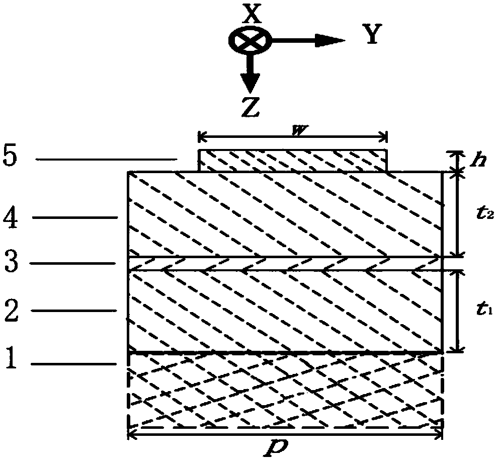
[0026] The parameters of a periodic structure of the filter are p=2000nm, w=1000nm, t 1 = t 2 =3000nm, h=230nm, ambient temperature is 300K, graphene relaxation time is 1ps, dielectric film layer and grating layer material are tantalum pentoxide (refractive index 2.0), substrate is silicon dioxide (refractive index 1.44) .
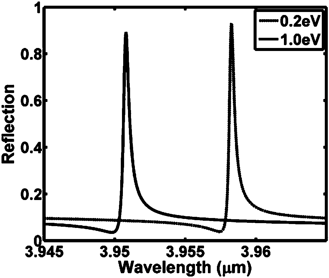
[0027] Using the rigorous coupled wave analysis method, the calculated reflection results are as follows figure 2 As shown, the reflection bandwidth is less than 1.0nm, the tuning graphene Fermi energy is from 0.2eV to 1.0eV, and the corresponding reflection peak is tuned from 3.95825μm to 3.95079μm. It can be seen that the device can tune the reflection peak of the filter by changing the graphene Fermi energy.
Embodiment 2
[0029] The parameters of a periodic structure of the filter are p=2000nm, w=1000nm, t 1 = t 2 =3000nm, h=200nm or 260nm, ambient temperature is 300K, graphene relaxation time is 1ps, dielectric film layer and grating layer material are tantalum pentoxide (refractive index 2.0), substrate is silicon dioxide (refractive index 1.44).
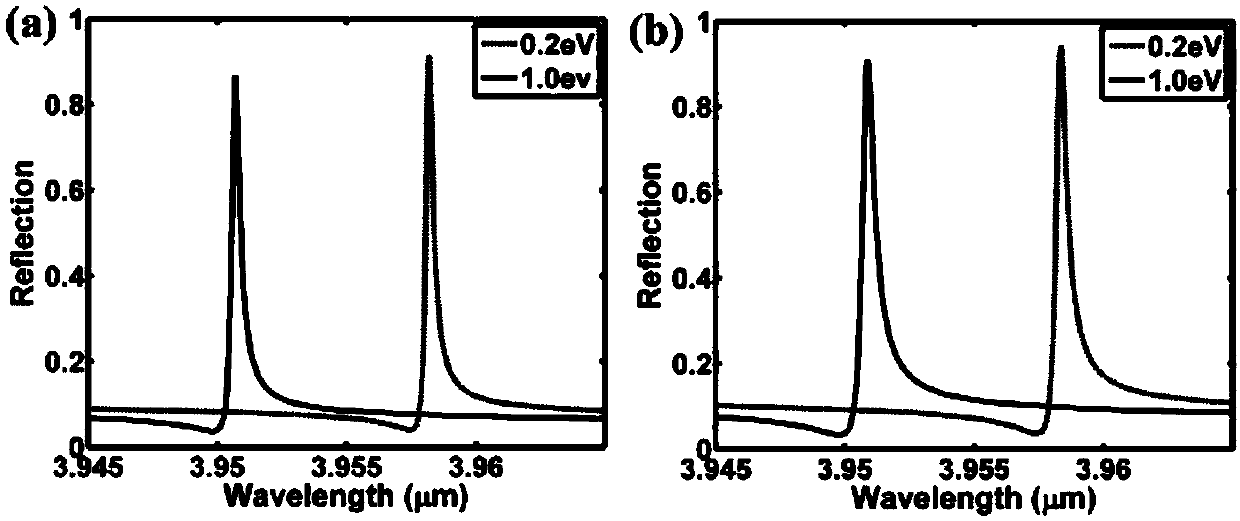
[0030] Using the rigorous coupled wave analysis method, the calculated reflection results are as follows image 3 As shown, the reflection bandwidth is still less than 1.0nm, and the tuning graphene Fermi energy is from 0.2eV to 1.0eV. When h=200nm, the corresponding reflection peak is tuned from 3.9582μm to 3.9507μm, see image 3 (a); when h=260nm, the corresponding reflection peak is tuned from 3.9583μm to 3.9509μm, see image 3 (b).
Embodiment 3
[0032] The parameters of a periodic structure of the filter are p=2000nm, w=800nm or 1200nm, t 1 = t 2 =3000nm, h=230nm, ambient temperature is 300K, graphene relaxation time is 1ps, dielectric film layer and grating layer material are tantalum pentoxide (refractive index 2.0), substrate is silicon dioxide (refractive index 1.44) .
[0033] Using the rigorous coupled wave analysis method, the calculated reflection results are as follows Figure 4 As shown, the reflection bandwidth is still less than 1.0nm, and the tuning graphene Fermi energy is from 0.2eV to 1.0eV. When w=800nm, the corresponding reflection peak is tuned from 3.95826μm to 3.95078μm, see Figure 4 (a); when w=1200nm, the corresponding reflection peak is tuned from 3.9583μm to 3.95082μm, see Figure 4 (b).
PUM
| Property | Measurement | Unit |
|---|---|---|
| thickness | aaaaa | aaaaa |
| width | aaaaa | aaaaa |
| thickness | aaaaa | aaaaa |
Abstract
Description
Claims
Application Information


