
A kind of circuit board processing method

A processing method and circuit board technology, applied in the direction of printed circuit, printed circuit manufacturing, electrical components, etc., can solve the problem of excessive metal debris or glass fiber cloth debris, reduce the efficiency of cutting and edging copper clad laminates, and increase the processing cycle of copper clad laminates and other problems, to achieve the effect of improving cutting and edging efficiency, facilitating movement and cutting

Active Publication Date: 2019-10-11
高唐融知融智科技服务有限公司
View PDF6 Cites 0 Cited by
  • Summary
  • Abstract
  • Description
  • Claims
  • Application Information

AI Technical Summary

Problems solved by technology

[0004] When the PCB circuit board needs to be processed into a circular shape, the copper clad laminate is often cut by stamping, and the section formed by stamping will have more deformation, which will cause metal debris or glass fiber remaining on the section of the copper clad laminate. There are more cloth debris, which increases the risk of scratching the copper clad laminate; after the copper clad laminate is cut, it is generally necessary to take out the cut copper clad laminate for cross-section grinding. In the process of transferring the copper clad laminate, the processing of the copper clad laminate will be increased cycle, which will reduce the efficiency of cutting and edging of copper clad laminates

Method used


Image

  • A kind of circuit board processing method
  • A kind of circuit board processing method

Examples


Embodiment Construction

[0021] Further detailed explanation through specific implementation mode below:

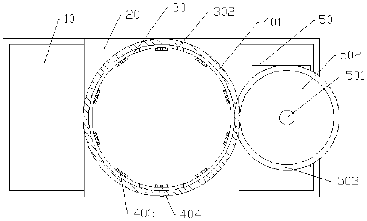
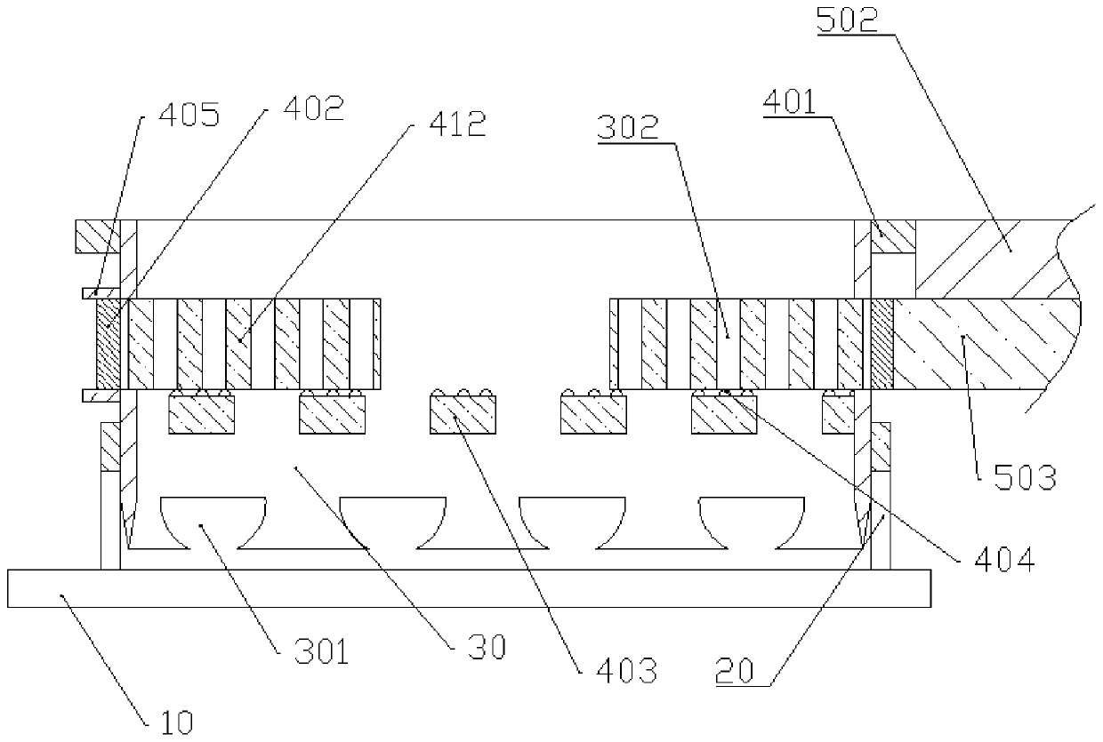
[0022] The reference numerals in the accompanying drawings include: cutting table 10, bracket 20, cutter 30, incision 301, grinding through groove 302, first ring gear 401, second ring gear 402, grinding teeth 412, wedge 403, ball 404 , the limit ring 405 , the motor 50 , the transmission shaft 501 , the first driving gear 502 , and the second driving gear 503 .

[0023] The cutting device in the embodiment is basically as attached figure 1 And attached figure 2 Shown: including cutting table 10, cutting mechanism and grinding mechanism.

[0024] Cutting mechanism comprises annular cutting knife 30 and support 20, and support 20 is welded on the cutting table 10, and cutting knife 30 is vertically slidably installed on the support 20, and the lower end of cutting knife 30 is provided with blade, and one end of cutting knife 30 blade Opposite to the upper surface of the cutting table 10 , a pl...


PUM


Abstract

The invention relates to the field of circuit boards and particularly discloses a circuit board processing method. A cutting device is adopted in the method and can cut a copper-clad plate, meanwhilecan also grind a cut cross section, can effectively reduce metal chippings or glass fiber chippings attached to the cross section, can reduce the possibility that the copper-clad plate is scratched and can fully ensure the quality of a finally obtained round copper-clad plate.

Description

technical field [0001] The invention belongs to the field of circuit boards, and in particular relates to a circuit board processing method. Background technique [0002] The Chinese name of PCB is printed circuit board, also known as printed circuit board. It is an important electronic component, a support for electronic components, and a carrier for electrical connections of electronic components. The processing process of the formed printed circuit board is complicated, including cutting, drilling, copper sinking, pattern transfer, pattern electroplating, stripping, etching, green oil, characters, gold-plated fingers, forming, testing and final inspection. Processing steps, wherein each step also includes a number of small processing steps, such as the cutting step, the specific processing is to cut the copper clad laminate, the cutting step can make the size of the copper clad laminate and the printed circuit after processing The size of the board is adapted, and then t...

Claims


Application Information

Patent Timeline
Patent Type & Authority Patents(China)
IPC IPC(8): H05K3/00
Inventor 胡红生
Owner 高唐融知融智科技服务有限公司
Learn More