Method of depositing a perovskite material

A technology of perovskite materials and inorganic materials, applied in metal material coating technology, liquid chemical plating, electrolytic capacitors, etc., can solve the problems of reducing the efficiency of silicon cells and increasing processing costs

Active Publication Date: 2018-02-27
OXFORD PHOTOVOLTAICS
View PDF4 Cites 16 Cited by
  • Summary
  • Abstract
  • Description
  • Claims
  • Application Information

AI Technical Summary

Problems solved by technology

While this approach avoids the problems associated with the deposition of perovskite cells, it would require mechanical polishing of conventional crystalline silicon solar cells to create a flat surface, increasing processing costs and reducing the efficiency of silicon cells

Method used


Image

  • Method of depositing a perovskite material
  • Method of depositing a perovskite material
  • Method of depositing a perovskite material

Examples


Embodiment Construction

[0075] definition

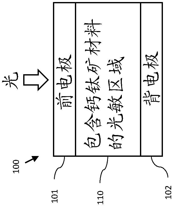
[0076] The term "photosensitive" as used herein refers to a region, layer or material capable of photoelectrically responding to light. A photosensitive region, layer or material is thus capable of absorbing energy carried by photons of light, which subsequently leads to the generation of electricity (for example by generating electron-hole pairs or excitons).

[0077] The term "conformable" as used herein refers to an object that is substantially the same in form or shape as another object. Thus, "conformal layer" as used herein refers to a layer of material that conforms to the contours of the surface on which it is formed. In other words, the morphology of the layer is such that the thickness of the layer is approximately constant over most of the interface between the layer and the surface on which the layer is formed.

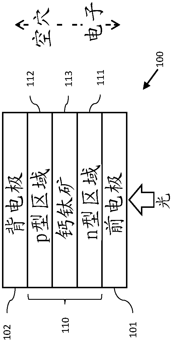
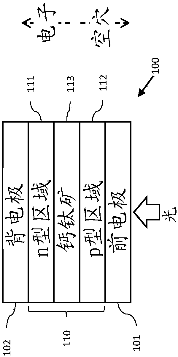
[0078] The term "perovskite" as used herein refers to a 3A material with a structurally related three-dimensional crystal structure...


PUM

PropertyMeasurementUnit
surface roughnessaaaaaaaaaa
thicknessaaaaaaaaaa
surface roughnessaaaaaaaaaa

Abstract

There is provided a method of producing a photovoltaic device comprising a photoactive region comprising a layer of perovskite material, wherein the layer of perovskite material is disposed on a surface that has a roughness average (Ra) or root mean square roughness (R rms) of greater than or equal to 50 nm. The method comprises using vapour deposition to deposit a substantially continuous and conformal solid layer comprising one or more initial precursor compounds of the perovskite material, and subsequently treating the solid layer with one or more further precursor compounds to form a substantially continuous and conformal solid layer of the perovskite material on the rough surface. There is also provided a photovoltaic device comprising a photoactive region comprising a layer of perovskite material disposed using the method.

Description

technical field [0001] The present invention relates to a method of depositing a conformal layer of photosensitive perovskite material onto a rough or textured surface, and a photovoltaic device comprising a conformal layer of photosensitive perovskite material disposed on a rough or textured surface. Background technique [0002] Over the past forty years or so, there has been growing recognition of the need to replace fossil fuels with safer sustainable energy sources. New energy supplies must also have low environmental impact, be highly efficient and be easy to use and inexpensive to produce. To this end, solar energy is considered one of the most promising technologies, however, the high cost of manufacturing devices that capture solar energy, including high material costs, has historically hindered its widespread use. [0003] Each solid has its own characteristic band structure that determines a wide range of electrical properties. Electrons are able to transition f...

Claims


Application Information

Patent Timeline
Patent Type & Authority Applications(China)
IPC IPC(8): C23C18/12H01L51/00H01L51/44H01L51/42
CPCC23C18/1204H01L31/0725H01L31/0745H10K71/164H10K30/87H10K30/82H10K30/00Y02E10/549Y02E10/542Y02P70/50H10K30/151H10K2102/103H10K85/50H01L2031/0344H01G9/0036H01G9/2009H01L31/02363H01L31/074
Inventor B·A·卡米诺L·M·佩雷斯
Owner OXFORD PHOTOVOLTAICS
Why Eureka
Try Eureka