
Surface treatment method for inhibiting overplating of electronic ceramic element and electronic ceramic element

An electronic ceramic component and surface treatment technology, applied in the field of electronic ceramics, can solve the problems of easy plating of nickel layer and tin layer on the surface of the product, poor appearance of the product, conduction and short circuit of the surface layer, etc. The effect of increasing surface resistance

Inactive Publication Date: 2018-03-06
HUNAN JIAYEDA ELECTRONICS
View PDF3 Cites 1 Cited by
  • Summary
  • Abstract
  • Description
  • Claims
  • Application Information

AI Technical Summary

Problems solved by technology

Chip components are usually composed of component substrates, internal electrodes and terminal electrodes. In order to improve the solderability of the components, a layer of nickel and a layer of tin should be plated on the surface of the terminal electrodes, but the surface of the product is also easy to be plated during the electroplating process. The upper nickel layer and tin layer will cause poor appearance of the product and conduction and short circuit of the surface layer, resulting in poor application of the product. Therefore, there is an urgent need for a surface treatment method to inhibit the creeping plating of electronic ceramic components

Method used


Image

  • Surface treatment method for inhibiting overplating of electronic ceramic element and electronic ceramic element
  • Surface treatment method for inhibiting overplating of electronic ceramic element and electronic ceramic element
  • Surface treatment method for inhibiting overplating of electronic ceramic element and electronic ceramic element

Examples


Embodiment 1

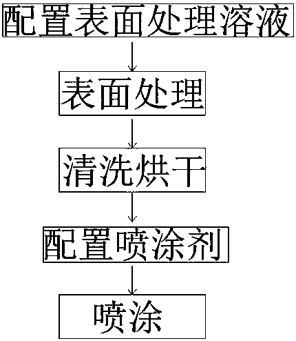
[0033] refer to figure 1 A surface treatment method for suppressing creep plating of electronic ceramic components, comprising the following steps:

[0034] S1: Prepare a surface treatment solution: mix the mixed material with water evenly to obtain a surface treatment solution. The mixed material includes perchloric acid and a catalyst;

[0035] S2: Surface treatment: soak the electronic ceramic components in the surface treatment solution to form a spray coating on the surface of the electronic ceramic components;

[0036] S3: Cleaning and drying: cleaning the surface residues of the electronic ceramic components treated in step S2, and drying the electronic ceramic components;

[0037] S4: Prepare spraying agent: Propionaldehyde, propane, propylene and ethylene are selected as raw materials and mixed. %, ethylene 15% to 25%;

[0038] S5: Spraying: Spraying is carried out by thermal spraying method, and the temperature is lowered after spraying.

[0039] The time of soak...

Embodiment 2

[0051] S1: Prepare a surface treatment solution: mix the mixed material with water evenly to obtain a surface treatment solution. The mixed material includes perchloric acid and a catalyst;

[0052] S2: Surface treatment: soak the electronic ceramic components in the surface treatment solution to form a spray coating on the surface of the electronic ceramic components;

[0053] S3: Cleaning and drying: cleaning the surface residues of the electronic ceramic components treated in step S2, and drying the electronic ceramic components;

[0054] S4: Prepare spraying agent: a-cyanoacrylate, propionaldehyde, propane, propylene and ethylene are used as raw materials to mix and make, and the components and the concentration of each component are 20% to 40% of propionaldehyde and 20% to 30% of propane. %, 5% to 10% of propylene, 10% to 20% of ethylene, 10% to 30% of a-cyanoacrylate;

[0055] S5: Spraying: Spraying is carried out by thermal spraying method, and the temperature is lower...


PUM


Abstract

The invention discloses a surface treatment method for inhibiting overplating of an electronic ceramic element and the electronic ceramic element. The method comprises the following steps: preparing asurface treatment solution, namely, uniformly mixing mixed materials and water to obtain the surface treatment solution, wherein the mixed materials include a perchloric acid and a catalyst; carryingout surface treatment, namely, soaking the electronic ceramic element in the surface treatment solution in order to generate a plating layer on the surface of the electronic ceramic element; washingand drying, namely, washing surface residues of the treated electronic ceramic element, and drying the electronic ceramic element; preparing a spraying agent, namely, mixing raw materials including propionaldehyde, propane, propylene and ethylene to obtain the spraying agent; and spraying, namely, spraying through a thermal spraying method. According to the method, a high-resistivity protecting film is formed on the product surface, so that the surface resistance of a product is increased, and as a result, the electronic ceramic element product is inhibited from overplating during electroplating; and the flame retardance of the plating layer is improved, and thus the fire is avoided to a certain extent.

Description

technical field [0001] The invention relates to the technical field of electronic ceramics, in particular to a surface treatment method for inhibiting the scaling of electronic ceramic components. Background technique [0002] At present, electronic ceramics can use electric and magnetic ceramics in the electronics industry. Electronic ceramics are ceramics with new functions obtained through precise control of surface, grain boundary and size structure. Can be widely used in energy, household appliances, automobiles, etc. With the rapid development of the electronic information industry, chip electronic ceramic components have been widely used, and more and more components have achieved chip and miniaturization. Chip components are usually composed of component substrates, internal electrodes and terminal electrodes. In order to improve the solderability of the components, a layer of nickel and a layer of tin should be plated on the surface of the terminal electrodes, but ...

Claims


Application Information

Patent Timeline
Patent Type & Authority Applications(China)
IPC IPC(8): C04B41/89C04B35/453C04B35/622
CPCC04B35/453C04B35/622C04B41/52C04B41/89C04B41/50C04B41/4535C04B41/4556C04B41/46
Inventor 戴承萍
Owner HUNAN JIAYEDA ELECTRONICS
Learn More