Manufacturing method of array substrate and array substrate

An array substrate and base technology, which is applied to the preparation of array substrates and the field of array substrates, can solve problems such as large slope angle of metal patterns, and achieve the effects of reducing occlusion, reducing differences and shortening preparation time.

Active Publication Date: 2018-03-09
HEFEI XINSHENG OPTOELECTRONICS TECH CO LTD +1
View PDF5 Cites 7 Cited by
  • Summary
  • Abstract
  • Description
  • Claims
  • Application Information

AI Technical Summary

Problems solved by technology

[0006] The present invention aims at the above-mentioned deficiencies existing in the prior art, and provides a preparation method of an array substrate and an array substrate, which are used to at least partially solve the problem that the metal pattern of the existing array substrate has a large slope angle

Method used


Image

  • Manufacturing method of array substrate and array substrate
  • Manufacturing method of array substrate and array substrate
  • Manufacturing method of array substrate and array substrate

Examples


Embodiment Construction

[0037] In order for those skilled in the art to better understand the technical solution of the present invention, a method for preparing an array substrate and the array substrate provided by the present invention will be described in detail below with reference to the accompanying drawings.

[0038] An embodiment of the present invention provides a method for preparing an array substrate, combining Figure 2a to Figure 3 As shown, the method includes:

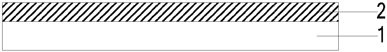
[0039] Step 1, depositing a metal thin film 2 on a substrate 1 .

[0040] Specifically, such as Figure 2a As shown, the metal thin film 2 can be deposited on the substrate 1 by physical vapor deposition, such as magnetron sputtering.

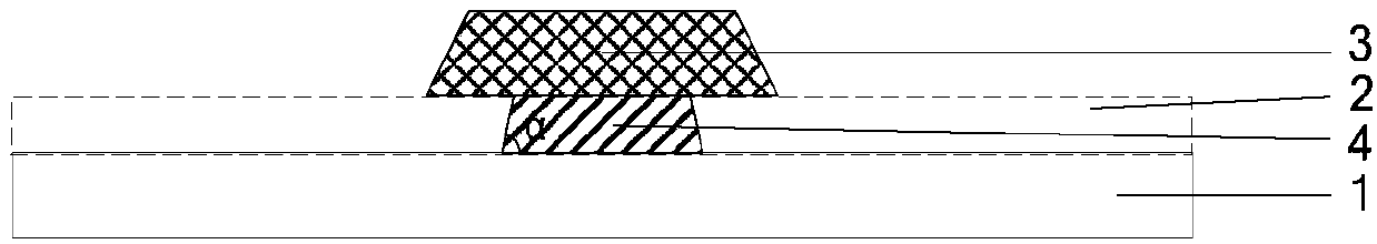
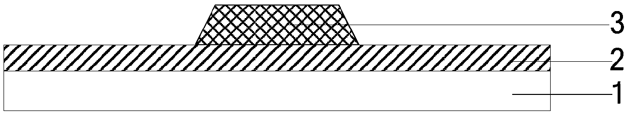
[0041] Step 2, forming a first mask pattern 3 on the substrate 1 on which the metal thin film 2 is formed by a photolithography process.

[0042] Specifically, such as Figure 2b As shown, a photoresist is coated on the surface of the substrate 1 on which the metal thin film 2 is formed, a...


PUM

PropertyMeasurementUnit
angleaaaaaaaaaa

Abstract

The invention provides a manufacturing method of an array substrate and the array substrate. The method includes the steps of conducting primary etching on a metal thin film through an etching technology by means of a first mask figure, and conducting secondary etching on the metal thin film through the etching technology by means of a second mask figure to form a metal figure, wherein the width of the second mask figure is smaller than that of the first mask figure. By means of the method, the shielding effect of the mask figure on etching liquid can be reduced, the slope angle of the metal figure can be reduced, the thickness of an insulating layer depositing on the edge position of the metal figure can be increased in the subsequent manufacturing process of the array substrate, the electrostatic breakdown generated on the edge position of the metal figure is avoided, and the yield of the array substrate is increased, and the manufacturing method of the array substrate is simple in process, low in cost and short in manufacturing time.

Description

technical field [0001] The invention relates to the field of display technology, in particular to a method for preparing an array substrate and the array substrate. Background technique [0002] The array substrate includes a driver module, a metal pattern (that is, a signal line), a thin film transistor and a pixel electrode. The metal pattern is connected to the driver module and the thin film transistor, and the pixel electrode is connected to the thin film transistor. The driver module adjusts the voltage of the thin film transistor through the metal pattern to adjust The voltage of the pixel electrode. The preparation method of existing metal pattern is as figure 1 As shown, first a metal film 2 is deposited on a substrate 1, then a first mask pattern 3 is formed on the metal film 2 by a photolithography process, and then the parts not covered by the first mask pattern 3 are etched by a wet etching process. The metal thin film 2, and finally the first mask pattern 3 i...

Claims


Application Information

Patent Timeline
Patent Type & Authority Applications(China)
IPC IPC(8): H01L21/77H01L27/12
CPCH01L27/124H01L27/1288
Inventor 苏同上刘军王东方周斌程磊磊成军王庆贺鲍俊袁广才
Owner HEFEI XINSHENG OPTOELECTRONICS TECH CO LTD
Why Eureka
Try Eureka