Semiconductor device with separated planar field plate structure and manufacturing method thereof

A manufacturing method and semiconductor technology, applied in semiconductor/solid-state device manufacturing, semiconductor devices, transistors, etc., can solve problems such as limiting the final characteristics of high-voltage devices, achieve the effects of shortening the current path in the drift region, achieving compatibility, and improving performance

Inactive Publication Date: 2018-03-09
CSMC TECH FAB2 CO LTD
View PDF7 Cites 3 Cited by
  • Summary
  • Abstract
  • Description
  • Claims
  • Application Information

AI Technical Summary

Problems solved by technology

Since the field plate is inseparable from the polysilicon of the gate, the longer the field plate of the higher voltage device, the greater the gate charge (Qgd), which limits the final characteristics of the high voltage device

Method used


Image

  • Semiconductor device with separated planar field plate structure and manufacturing method thereof
  • Semiconductor device with separated planar field plate structure and manufacturing method thereof
  • Semiconductor device with separated planar field plate structure and manufacturing method thereof

Examples


Embodiment 1

[0059] In order to solve the problems in the prior art, the invention provides a method for manufacturing a semiconductor device, such as image 3 As shown, it includes the following main steps:

[0060] Step S1, providing a semiconductor substrate, forming a source, a drain, and a gate on the semiconductor substrate, and forming a drift region in the semiconductor substrate between the gate and the drain,

[0061] Step S2, forming a first dielectric layer to cover the surface of the semiconductor substrate and the source, drain and gate,

[0062] Step S3 , forming a first field plate layer on the first dielectric layer, and the first field plate layer is at least partially located above the drift region and close to the side of the gate.

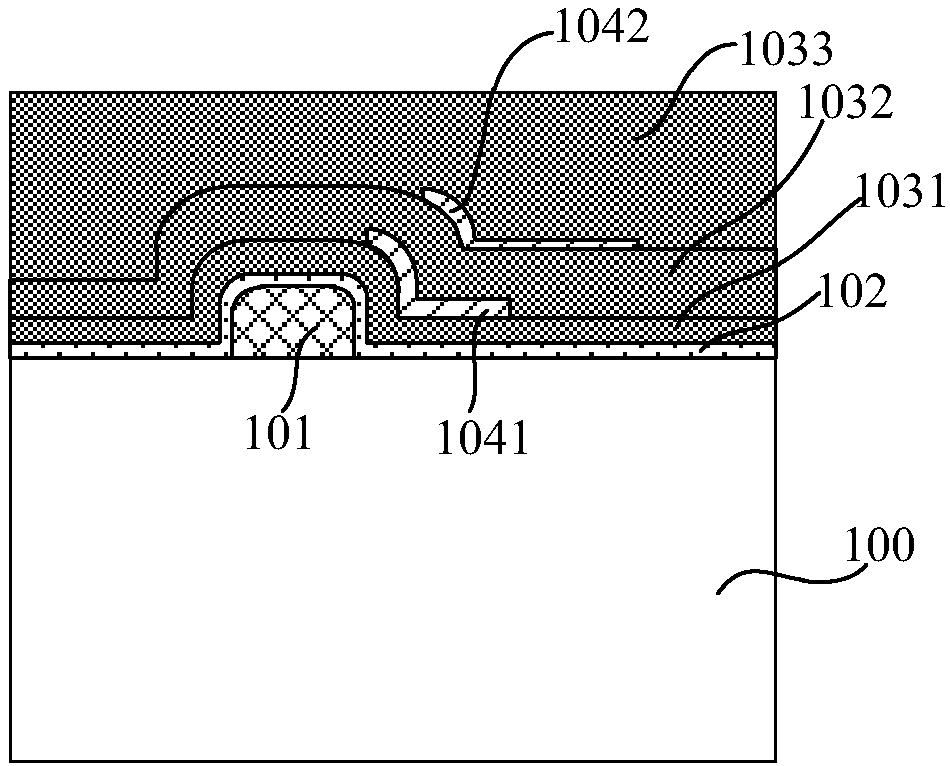
[0063] According to the manufacturing method of the present invention, during the process of depositing the dielectric layer, the steps of depositing the dielectric layer and forming the field plate layer are alternately performed to form ...

Embodiment 2

[0130] The present invention also provides a semiconductor device, which can be the semiconductor device prepared by using the method in the first embodiment above.

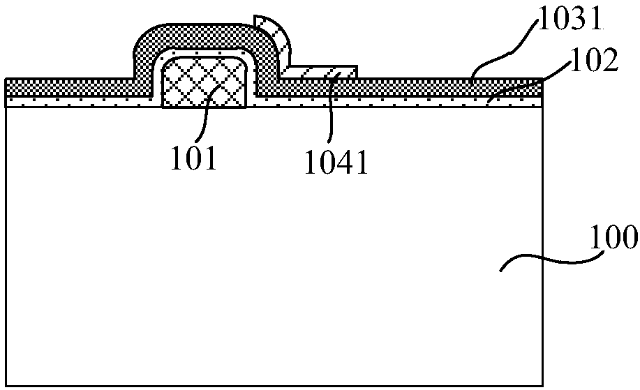
[0131] In one embodiment, as Figure 1A As shown, the semiconductor device of the present invention includes:

[0132] A semiconductor substrate 100, on which a source, a drain, and a gate 101 are formed, and a drift region is formed in the semiconductor substrate between the gate 101 and the drain;

[0133] The first dielectric layer 1031 covers the surface of the semiconductor substrate 100 and the source, drain and gate 101;

[0134] The first field plate layer 1041 is formed on the first dielectric layer 1031, the first field plate layer is at least partially located above the drift region and close to the side of the gate 101, for example, the The first field plate layer 1041 is partly located above the gate 101, and the first field plate layer 1041 includes a part located on the gate and a part located on ...


PUM

PropertyMeasurementUnit
Thicknessaaaaaaaaaa

Abstract

The invention provides a semiconductor device with a separated planar field plate structure and a manufacturing method thereof. The method comprises: step 1, providing a semiconductor substrate, forming a source, a drain and a gate on the semiconductor substrate, and forming a drift region in the semiconductor substrate between the gate and the drain; step 2, forming a first dielectric layer to cover the surface of the semiconductor substrate, the source, the drain and the gate; and step 3, forming a first field plate layer on the first dielectric layer, at least part of the first field platelayer being located above the drift region and close to the gate. According to the manufacturing method, the steps of depositing the dielectric layer and forming the field plate layer are alternatelyperformed to form a separated planar field plate structure comprising one, two or more field plate layers to achieve the advantage of compatibility between process platforms. The formed separated planar field plate structure shortens the current path of the drift region and improves the performance of the device.

Description

technical field [0001] The invention relates to the technical field of semiconductors, in particular to a semiconductor device with a split planar field plate structure and a manufacturing method thereof. Background technique [0002] The traditional high-voltage device structure usually adjusts the polysilicon length of the gate, expands the polysilicon to the drain direction to act as a field plate, and the field plate depletes the drift region to form a depletion layer, thus increasing the width of the lateral depletion layer, thereby improving Withstand voltage (that is, breakdown voltage). In addition, it is necessary to configure a suitable field plate oxide layer below the field plate to form a field plate structure, and the field plate oxide layer generally introduces an additional oxide layer between the drain and the gate in the drift region, which brings The negative effects of the technology limit the compatibility of the process and the characteristics of the c...

Claims


Application Information

Patent Timeline
IPC IPC(8): H01L29/78H01L29/06H01L29/40H01L21/336
CPCH01L29/0603H01L29/0684H01L29/404H01L29/66568H01L29/78
Inventor 罗泽煌
Owner CSMC TECH FAB2 CO LTD
Why Eureka
Try Eureka