Manufacturing method of contact image sensor

A technology of an image sensor and a manufacturing method, which can be applied to radiation control devices and other directions, and can solve the problems that the structural performance of CIS needs to be improved.

Inactive Publication Date: 2018-03-13
HUAIAN IMAGING DEVICE MFGR CORP
View PDF3 Cites 6 Cited by
  • Summary
  • Abstract
  • Description
  • Claims
  • Application Information

AI Technical Summary

Problems solved by technology

However, the performance of the CIS structure ma

Method used


Image

  • Manufacturing method of contact image sensor
  • Manufacturing method of contact image sensor
  • Manufacturing method of contact image sensor

Examples


Embodiment Construction

[0026] It can be seen from the background art that the performance of the CIS structure in the prior art needs to be improved.

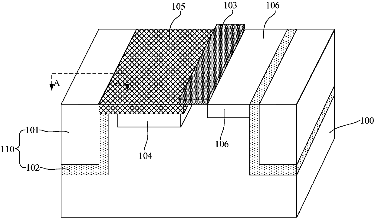
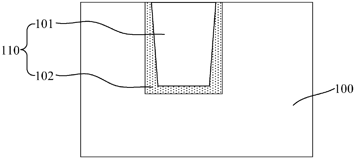
[0027] refer to figure 1 and figure 2 , figure 1 is a schematic diagram of the three-dimensional structure of a single pixel unit in the CIS structure, figure 2 for figure 1 A schematic diagram of a partial cross-sectional structure of the middle substrate and the isolation structure cut along the cutting line AA, the CIS structure includes:

[0028] The substrate 100 has several isolation structures 110 inside, and the area between adjacent isolation structures 110 is an active area, wherein the isolation structure 110 includes: a shallow trench isolation structure 101 and surrounding the shallow trench isolation structure 101. The P+ isolation well 102 of the trench isolation structure 101; the transfer gate 103 located on the partial surface of the active region of the substrate 100; the photodiode in the substrate 100 located on one side of...


PUM

PropertyMeasurementUnit
Thicknessaaaaaaaaaa

Abstract

Disclosed is a manufacturing method of a contact image sensor. The manufacturing method comprises the steps of providing a substrate; forming multiple trenches in the substrate; forming a doping layerat the bottoms and on the surfaces of the side walls of the trenches, wherein the doped ions in the doping layer are N type or P type ions; performing annealing treatment on the doping layer, enabling the doped ions in the doping layer to be diffused to the substrate at the bottoms and on the side walls of the trenches, and forming isolation doped wells which surround the trenches in the substrate; after the isolation doped wells are formed, forming isolation structures which are full of the trenches; and forming photodiodes in the substrate between adjacent isolation structures, wherein thephotodiodes are adjacent to the isolation doped wells. By virtue of the manufacturing method, damage of the substrate from lattice is lowered, thereby improving the performance of the manufactured contact image sensor.

Description

technical field [0001] The invention relates to the technical field of semiconductors, in particular to a method for manufacturing a contact image sensor. Background technique [0002] Image sensors are semiconductor devices that convert optical signals into electrical signals. The image sensor includes a photodiode for sensing light and a logic device for converting the sensed optical signal into an electrical signal. [0003] A contact image sensor (CIS, Contact Image Sensor) is a new type of image sensor composed of a photoelectric sensor array, an LED light source array, and a cylindrical lens array. These components are integrated in a strip-shaped square box, without additional optical accessories, and there is no problem of adjusting the optical path and depth of field. It has the advantages of simple structure, small size, and convenient application. In some applications, contact image sensors have incomparable advantages over complementary metal oxide (CMOS) image...

Claims


Application Information

Patent Timeline
IPC IPC(8): H01L27/146
Inventor 彭琬婷林宗德黄仁徳
Owner HUAIAN IMAGING DEVICE MFGR CORP
Why Eureka
Try Eureka