Whole-process traceable semiconductor test data recording method

A technology for testing data and recording methods, applied in the field of testing, which can solve problems such as data cannot be traced

Active Publication Date: 2018-03-16
SINO IC TECH
View PDF10 Cites 19 Cited by
  • Summary
  • Abstract
  • Description
  • Claims
  • Application Information

AI Technical Summary

Problems solved by technology

[0004] The present invention aims at the problem that data cannot be traced during the process from wafer testing to finished product testing, and proposes a whole-process traceable semiconductor testing data recording metho

Method used


Image

  • Whole-process traceable semiconductor test data recording method

Examples


Embodiment Construction

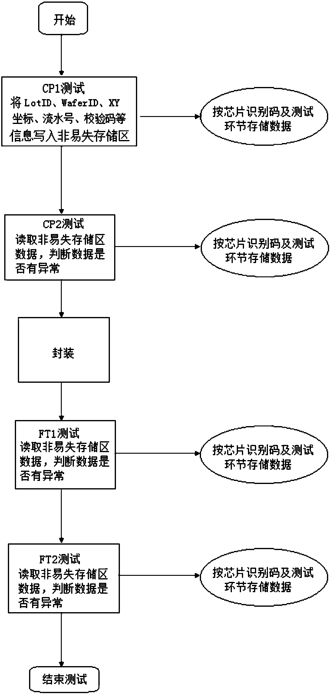
[0012] Wafer test CP: use test equipment to test the chip to be tested on the wafer; finished product test FT: use test equipment to test the packaged semiconductor chip; aging: the method of accelerating the damage of semiconductor chip by high temperature baking; test Detailed data, including the coordinates of the tested device on the original wafer, the name of the test item, the test value, the test condition, the judgment condition, etc.

[0013] In the process of the first test of the wafer, the present invention writes the unique identification code of the chip in the non-volatile storage area of ​​the tested chip, including but not limited to LotID (batch number), WaferID (wafer number), the Measure the XY coordinates, serial number, check code, etc. of the chip on the original wafer. At the same time, use this identification code plus the test link identification (such as the first test of the wafer, etc.) as the index information of the data file of the chip under te...


PUM


Abstract

The invention relates to a whole-process traceable semiconductor test data recording method. The unique identification code of each chip is written into a non-volatile memory area of the chip. Data iswritten into a database by taking the unique identification codes and test links as data index information. Through the identification codes and the test links, all test data can be indexed in the database, data generated in the whole test process can be tracked, and the change of the data can be monitored. For the same chip, data during wafer test and data of finished product test after packaging can be seen, and the data of each test link can be quickly and accurately obtained, so that the engineer can analyze the process data and screen out final qualified chips.

Description

technical field [0001] The invention relates to a detection technology, in particular to a whole-process traceable semiconductor test data recording method. Background technique [0002] The existing technical solution is to use LotID + WaferID of the wafer + the coordinates of each chip on the wafer to locate the data of each chip in the wafer testing process. In this way, if burn-in is performed in the wafer test, the coordinates of the semiconductor chip on the same wafer will not change after burn-in, so the test data can also be located by the coordinates. In the finished product testing process, the conventional practice is to number the finished chip and print or manually write it on the surface of the chip, so that the data can be traced through the chip number during multiple tests. However, the aging during multiple tests will make the ink on the surface of the chip blurred, and it may even cause the number to be unreadable if it is aged multiple times. Moreover,...

Claims


Application Information

Patent Timeline
IPC IPC(8): H01L21/66H01L21/67H01L23/544
CPCH01L21/67282H01L22/14H01L22/20H01L23/544H01L2223/5444
Inventor 邵嘉阳汤雪飞王玉龙王华罗斌凌俭波
Owner SINO IC TECH
Why Eureka
Try Eureka