Substrate structure and manufacturing method therefor

A manufacturing method and substrate technology, which are used in semiconductor/solid-state device manufacturing, electrical components, and electrical solid-state devices, etc., can solve the problem of increasing the connection path between electronic components and substrates, unable to meet the requirements of fine circuit wiring, and poor electrical characteristics of the substrate structure, etc. problem, to achieve the effect of combining rigidity, reduced substrate size, and high heat dissipation

Active Publication Date: 2018-03-27
PHOENIX PIONEER TECH
View PDF5 Cites 4 Cited by
  • Summary
  • Abstract
  • Description
  • Claims
  • Application Information

AI Technical Summary

Problems solved by technology

However, due to the conductivity of metal materials, when using a laminated structure of a substrate made of metal materials, it is necessary to consider the insulation design of the through holes between layers, and increase the connection path between electronic components and the substrate, thereby increasing the complexity of the process degree and make the electrical characteristics of the substrate structure poor
In addition, substrates using metal materials need to use laser drilling technology to form laser blind holes and mechanical drilling technology to form through holes in the same layer structure, so that the offset caused by alignment errors It cannot meet the wiring requirements of fine lines

Method used


Image

  • Substrate structure and manufacturing method therefor
  • Substrate structure and manufacturing method therefor
  • Substrate structure and manufacturing method therefor

Examples


Embodiment Construction

[0077] The content of the present invention will be explained by the following examples. The examples of the present invention are not intended to limit the present invention to be implemented in any specific environment, application or special method as described in the examples. Therefore, the descriptions about the embodiments are only used to illustrate the purpose of the present invention, not to limit the protection scope of the present invention. It should be noted that in the following embodiments and drawings, components not directly related to the present invention have been omitted and not shown; and the dimensional relationship between the components in the drawings is only for easy understanding, and is not used to limit the actual scale .

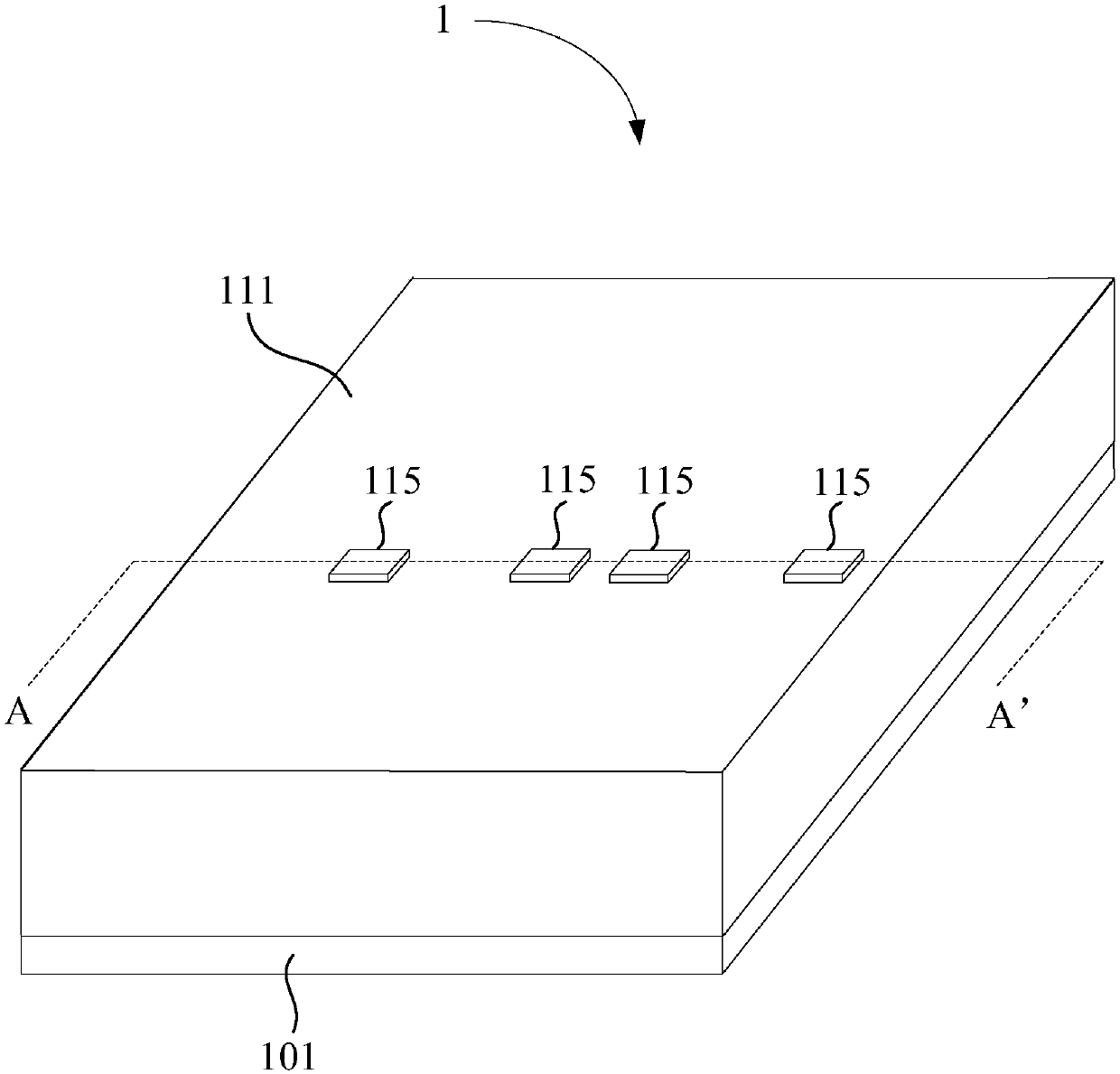
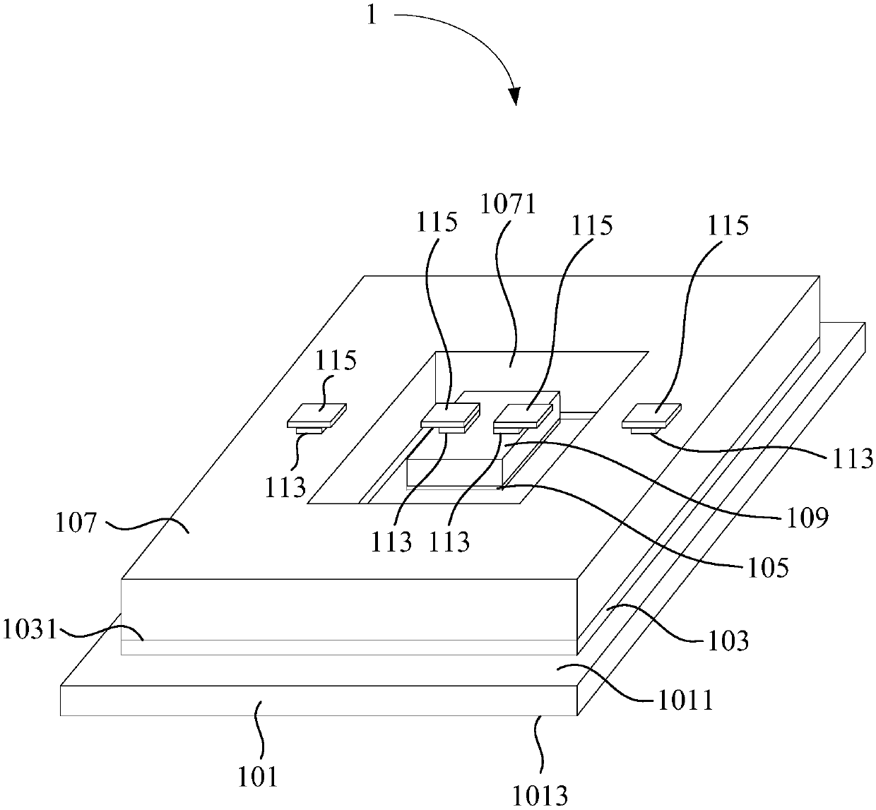
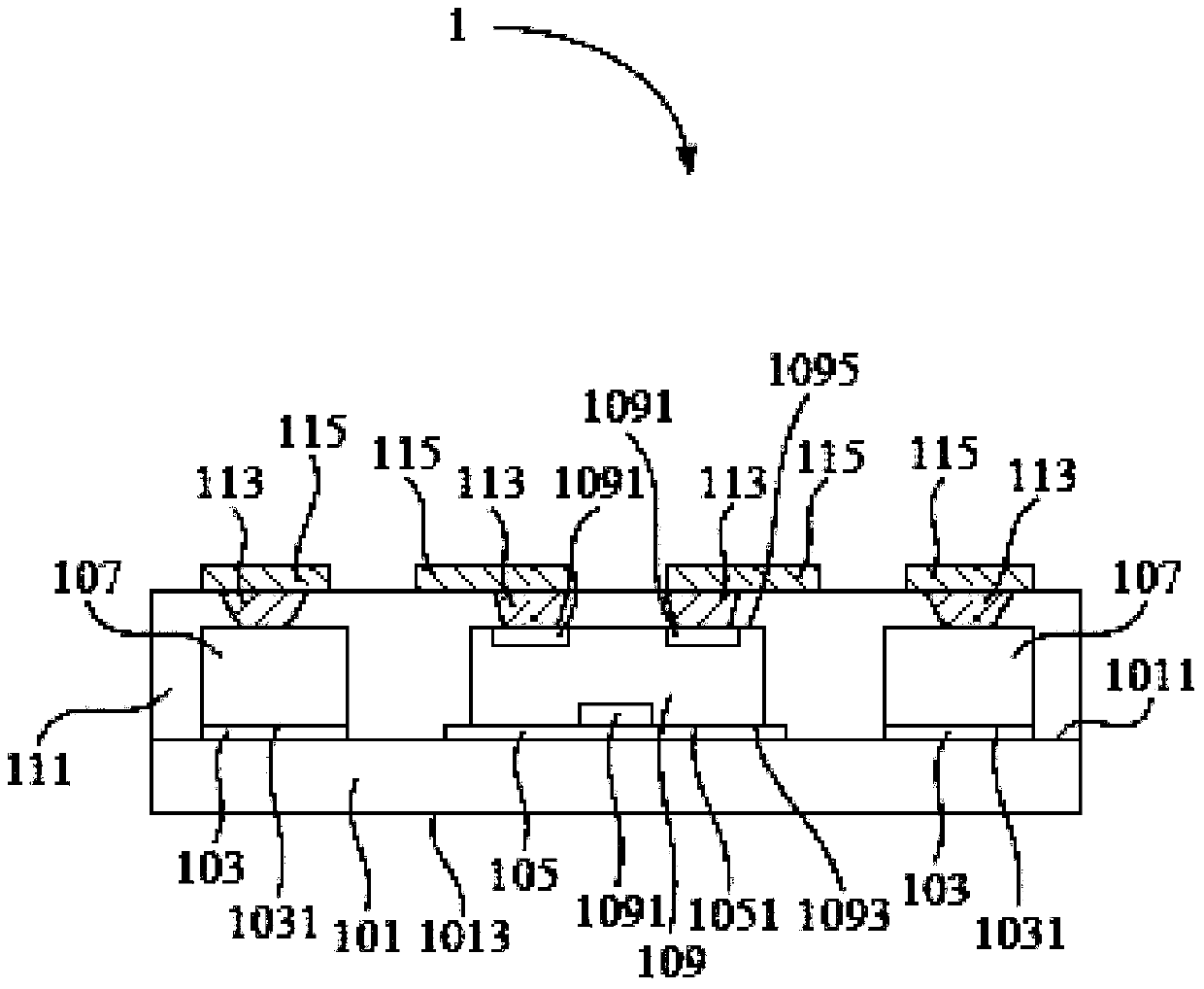
[0078] The first embodiment of the present invention is as figure 1 , figure 2 as well as image 3 shown. figure 1 is a schematic diagram of a substrate structure 1; figure 2 is a partial schematic diagram of the subs...


PUM


Abstract

Disclosed are a substrate structure and a manufacturing method therefor. The substrate structure comprises a metal substrate, a first connecting layer, a metal core layer, a second connecting layer, an inner connecting assembly and a dielectric material layer, wherein the first connecting layer is arranged on one surface of the metal substrate; the metal core layer is arranged on one surface of the first connecting layer, and has an opening; the second connecting layer is arranged on a partial surface of the metal substrate and positioned in the opening; the inner connecting assembly is arranged on one surface of the second connecting layer and positioned in the opening, and comprises multiple electrode cushions; and the dielectric material layer is arranged on the surface of the metal substrate and used for partially packaging the first connecting layer, the metal core layer, the second connecting layer and the inner connecting assembly. The metal core layer is electrically connectedwith one of the electrode cushions through the metal substrate, the first connecting layer and the second connecting layer.

Description

technical field [0001] The invention relates to the technical field of microelectronic structures, in particular to a semiconductor substrate structure and a manufacturing method thereof. Background technique [0002] In the new generation of electronic products, users not only pursue lighter, thinner and smaller, but also require them to have multi-function and high performance. Therefore, manufacturers of electronic products must accommodate more electronic components in a limited area of ​​an integrated circuit (IC) to meet the requirements of high density and miniaturization. Accordingly, electronic product manufacturers have developed a new packaging technology to embed electronic components in the substrate, thereby greatly reducing the packaging volume of integrated circuits, and shortening the connection path between electronic components and substrates, in order to meet the light, thin, short and multi-functional electronic products. the trend of. [0003] Under t...

Claims


Application Information

Patent Timeline
Patent Type & Authority Applications(China)
IPC IPC(8): H01L23/14H01L23/498H01L21/48
CPCH01L21/4853H01L23/142H01L23/49838H01L2224/18
Inventor 许诗滨
Owner PHOENIX PIONEER TECH
Why Eureka
Try Eureka