Nitrogen-Containing Semiconductor Device
一种半导体、元件的技术,应用在含氮半导体元件领域,能够解决晶格差异、半导体层磊晶质量降低等问题,达到改善晶格结构、改善磊晶质量的效果
- Summary
- Abstract
- Description
- Claims
- Application Information
AI Technical Summary
Problems solved by technology
Method used
Image

Examples
Embodiment Construction
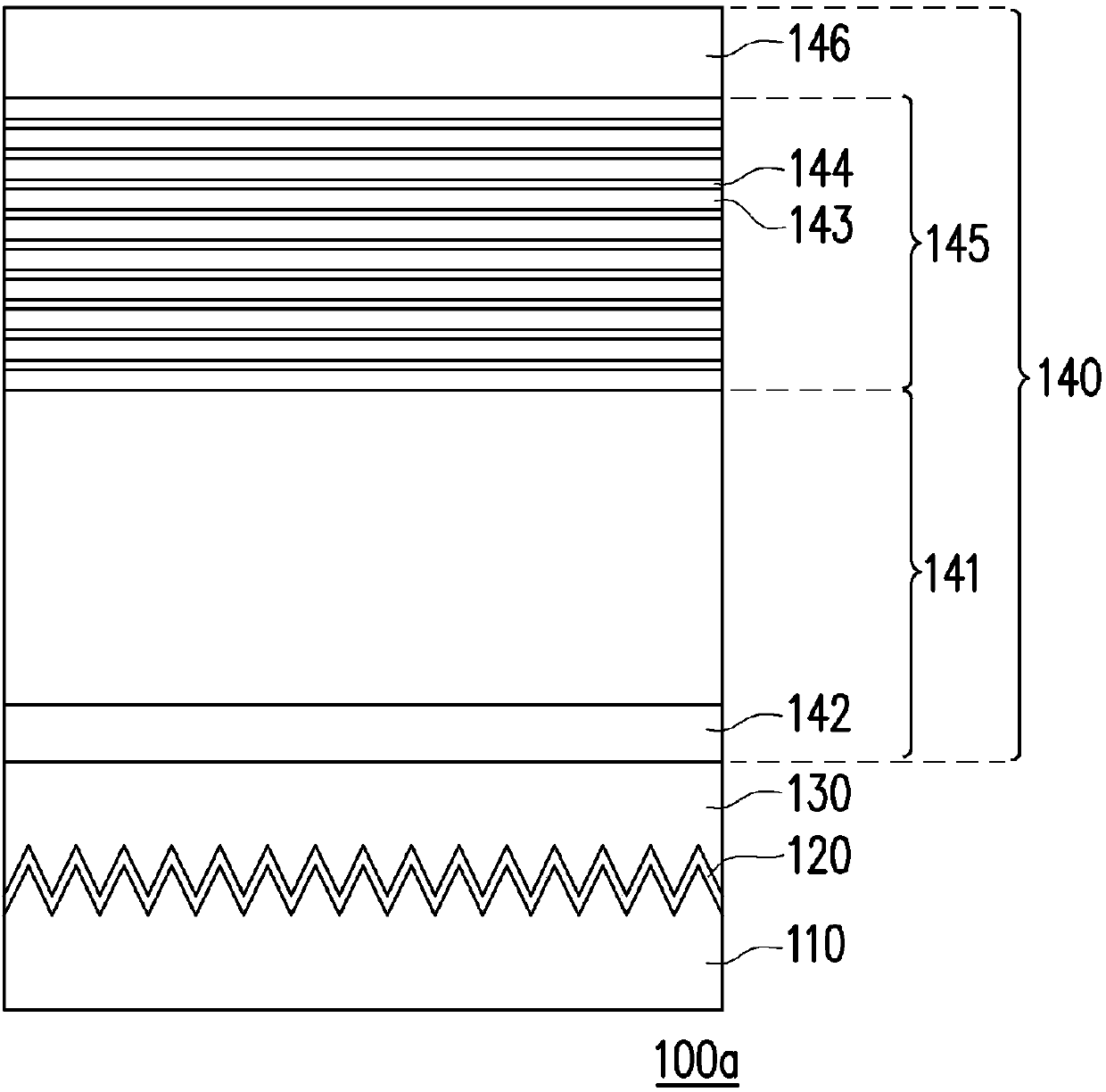
[0041] figure 1 is a schematic cross-sectional view of a nitrogen-containing semiconductor device according to the first embodiment of the present invention. Please refer to figure 1 The nitrogen-containing semiconductor device 100 a of this embodiment includes a substrate 110 , a first AlGaN buffer layer 120 , a second AlGaN buffer layer 130 and a semiconductor stack layer 140 . The first aluminum gallium nitride buffer layer 120 is disposed on the substrate 110, and the chemical formula of the first aluminum gallium nitride buffer layer 120 is Al x Ga 1-x N, where 0≦x≦1. In particular, the first AlGaN buffer layer 120 of this embodiment is doped with a concentration exceeding 5×10 17 cm -3 Oxygen with concentrations exceeding 5 x 10 17 cm -3 At least one of the two carbons. The second AlGaN buffer layer 130 is disposed on the first AlGaN buffer layer 120, and the chemical general formula of the second AlGaN buffer layer 130 is Al y Ga 1-y N, where 0≦y≦1. The semic...
PUM
 Abstract
Description
Claims
Application Information
 - R&D
- Intellectual Property
- Life Sciences
- Materials
- Tech Scout
- Unparalleled Data Quality
- Higher Quality Content
- 60% Fewer Hallucinations
Browse by: Latest US Patents, China's latest patents, Technical Efficacy Thesaurus, Application Domain, Technology Topic, Popular Technical Reports.
© 2025 PatSnap. All rights reserved.Legal|Privacy policy|Modern Slavery Act Transparency Statement|Sitemap|About US| Contact US: help@patsnap.com