Fan-out-shaped packaging structure of large power MOSFET and manufacturing technology

A packaging structure, high-power technology, applied in semiconductor/solid-state device manufacturing, electrical components, electric solid-state devices, etc., can solve problems such as space that is difficult to improve, and achieve low internal resistance, small stray parameters, and high power density than the effect

Pending Publication Date: 2018-03-30
华羿微电子股份有限公司
View PDF0 Cites 3 Cited by
  • Summary
  • Abstract
  • Description
  • Claims
  • Application Information

AI Technical Summary

Problems solved by technology

Traditional packaging has done a lot of optimization in order to meet these requirements, but due to the limitations of structure and materials, it has basically reached the limit, and it is difficult to have much room for improvement

Method used


Image

  • Fan-out-shaped packaging structure of large power MOSFET and manufacturing technology
  • Fan-out-shaped packaging structure of large power MOSFET and manufacturing technology
  • Fan-out-shaped packaging structure of large power MOSFET and manufacturing technology

Examples


Embodiment Construction

[0031] In order to make the object, technical solution and advantages of the present invention clearer, the present invention will be further described in detail below in conjunction with the accompanying drawings and embodiments. It should be understood that the specific embodiments described here are only used to explain the present invention, not to limit the present invention.

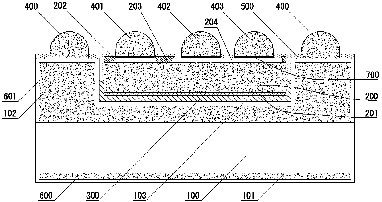
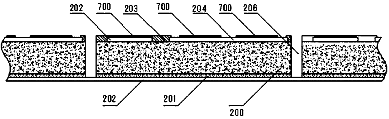
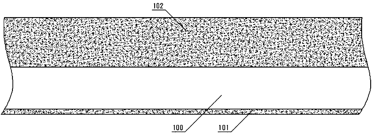
[0032] Embodiments of the present invention provide a fan-out packaging structure for high-power MOSFETs, such as figure 1 As shown, it includes a ceramic double-sided copper-clad substrate, a gold-plated layer 300, a single MOSFET chip 200 formed after dicing a high-power MOSFET wafer, and solder balls arranged in sequence from bottom to top. The ceramic double-sided copper-clad substrate It is provided with a lower embedded groove for a built-in single MOSFET chip 200, and the single MOSFET chip 200 is provided with a gate 202, a source 204 and a drain 201, and the solder balls include a first so...


PUM


Abstract

The invention discloses a fan-out-shaped packaging structure of a large power MOSFET. The structure comprises a ceramic double-sided copper-clad substrate, a gold-plated layer, a single MOSFET chip formed after carrying out scribing on a large power MOSFET wafer and solder balls which are successively arranged from bottom to top. The ceramic double-sided copper-clad substrate is provided with a lower embedded groove used for internally placing the single MOSFET chip. The single MOSFET chip is provided with a grid electrode, a source electrode and a drain electrode. The solder balls comprise first solder balls, a second solder ball, a third solder ball and a fourth solder ball. The first solder balls are located on two sides outside the lower embedded groove and are contacted with the gold-plated layer so as to lead out the drain electrode of a finished product. The second solder ball is located on the grid electrode and is used for leading out the grid electrode of the finished product. The third solder ball and the fourth solder ball are located on the source electrode and are used for leading out the source electrode of the finished product. The invention also discloses a manufacturing technology of the fan-out-shaped packaging structure of the large power MOSFET. In the invention, a lower internal resistance, a smaller stray parameter, better cooling performance and a largerpower density ratio of the MOSFET can be realized, simultaneously the structure and the technology are suitable for large scale mass production, and production cost is reduced.

Description

technical field [0001] The invention belongs to the field of semiconductor manufacturing, and in particular relates to a fan-out packaging structure of a high-power MOSFET and a manufacturing process thereof. Background technique [0002] The technical parameters and performance of metal oxide semiconductor field effect transistors (MOSFET) depend on the performance of the chip itself and the later packaging. After a wafer is produced, its parameters have been determined, but after the later packaging, the overall parameters will be affected. Some changes, which are mainly reflected in the introduction of DC parameters, AC parameters, thermal performance and stray inductance and stray capacitance. A good packaging form, under the premise of reasonable cost and suitable for mass production, will strive to enhance its thermal performance and humidity resistance level, without deteriorating its DC parameters, AC parameters, and stray parameters. [0003] The traditional metal ...

Claims


Application Information

Patent Timeline
Patent Type & Authority Applications(China)
IPC IPC(8): H01L23/31H01L23/367H01L23/488H01L21/56
CPCH01L21/561H01L23/31H01L23/367H01L23/488H01L2224/12105H01L2224/32245H01L2224/73267H01L2224/92244H01L2224/97H01L2924/15153H01L2224/83
Inventor 刘义芳
Owner 华羿微电子股份有限公司
Why Eureka
Try Eureka