A kind of three-dimensional memory and its preparation method

A memory, three-dimensional technology, applied in the direction of semiconductor devices, electrical solid-state devices, electrical components, etc., to achieve the effect of improving device performance

Active Publication Date: 2021-05-11
INST OF MICROELECTRONICS CHINESE ACAD OF SCI
View PDF10 Cites 0 Cited by
  • Summary
  • Abstract
  • Description
  • Claims
  • Application Information

AI Technical Summary

Problems solved by technology

[0004] In order to solve the above-mentioned technical problems, the present invention provides a three-dimensional memory and its preparation method, to solve the problem that the first dielectric layer closest to the substrate of the stacked structure constituting the step region reacts with the substrate in the subsequent process, so that the Problems with the formation of unnecessary oxidative structures in the

Method used


Image

  • A kind of three-dimensional memory and its preparation method
  • A kind of three-dimensional memory and its preparation method
  • A kind of three-dimensional memory and its preparation method

Examples


Embodiment Construction

[0051] The following will clearly and completely describe the technical solutions in the embodiments of the present invention with reference to the accompanying drawings in the embodiments of the present invention. Obviously, the described embodiments are only some, not all, embodiments of the present invention. Based on the embodiments of the present invention, all other embodiments obtained by persons of ordinary skill in the art without making creative efforts belong to the protection scope of the present invention.

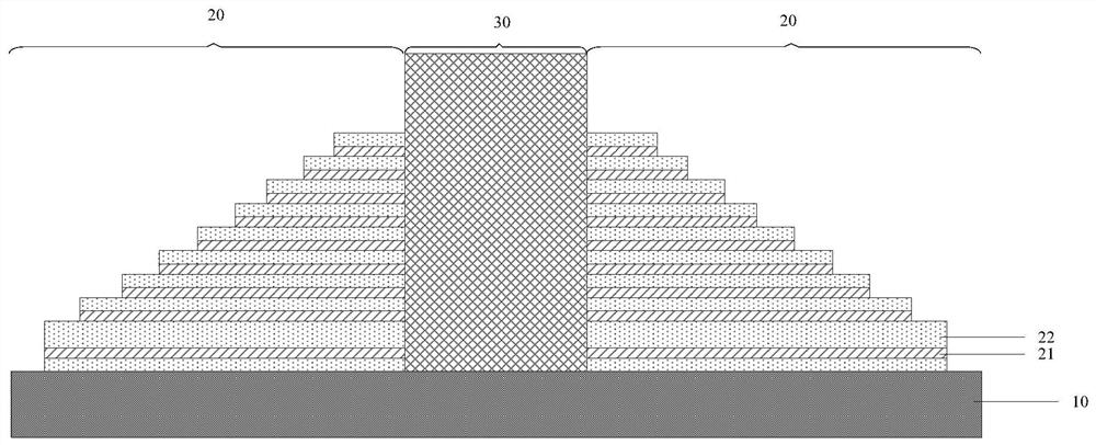
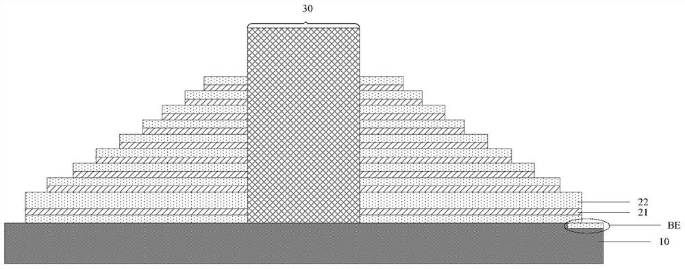
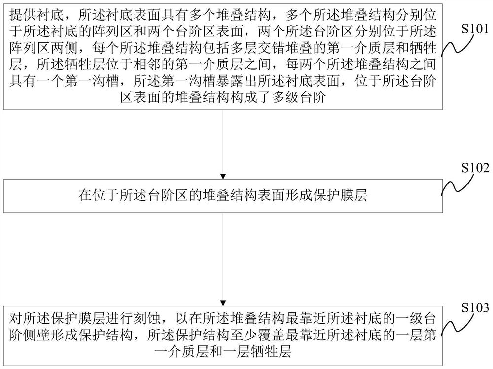
[0052] The embodiment of the present application provides a method for preparing a three-dimensional memory, such as image 3 shown, including:

[0053] S101: Provide a substrate, the surface of the substrate has multiple stacked structures, the multiple stacked structures are respectively located on the array area of ​​the substrate and the surface of two step areas, and the two step areas are respectively located on the surface of the array On both sides of t...


PUM


Abstract

The present application discloses a three-dimensional memory and a preparation method thereof. In the preparation method of the three-dimensional memory, after forming a stack structure located in the array area and a step area on the surface of the substrate, a protective film is formed on the surface of the stack structure located in the step area. layer, and etch the protective film layer. During the etching process, after the etching of the protective film layers of other steps is completed, a part of the protective film layer on the side wall of the first step closest to the substrate remains. This part of the remaining protective film layer becomes a protective structure attached to the sidewall of the first-level step closest to the substrate, thereby protecting the first dielectric layer and the sacrificial layer closest to the substrate, avoiding the In the subsequent preparation process, the first dielectric layer reacts with other contacts with the substrate, thereby avoiding the formation of unnecessary oxidation structures in the substrate, and improving the performance of the final three-dimensional memory. device performance.

Description

technical field [0001] The present application relates to the technical field of semiconductors, and more specifically, to a three-dimensional memory and a preparation method thereof. Background technique [0002] Memory is a memory device used to save information in modern information technology. With the increasing demand for integration and data storage density of various electronic devices, it is difficult for ordinary two-dimensional memory to further improve its integration and data storage density. Therefore, three-dimensional (3D) memory has emerged as the times require. [0003] Three-dimensional NAND (NAND) memory is a kind of three-dimensional flash memory. In its preparation process, a stacked structure is first deposited on the surface of a silicon substrate, and each stacked structure includes a multilayer interleaved first dielectric layer and a sacrificial layer, the sacrificial layer is located between adjacent first dielectric layers, refer to figure 1 , ...

Claims


Application Information

Patent Timeline
Patent Type & Authority Patents(China)
IPC IPC(8): H01L27/11578H01L27/11582
CPCH10B43/20H10B43/27
Inventor 赵治国霍宗亮李春龙叶甜春
Owner INST OF MICROELECTRONICS CHINESE ACAD OF SCI
Why Eureka
Try Eureka