Manufacture method of laser chip

A manufacturing method and laser technology, which are applied to the structure of optical waveguide semiconductors and other directions, can solve the problems of low yield of single-mode lasers and low yield of laser chips, and achieve the effect of saving costs and simplifying design steps.

Active Publication Date: 2018-04-03
HISENSE BROADBAND MULTIMEDIA TECH
View PDF6 Cites 4 Cited by
  • Summary
  • Abstract
  • Description
  • Claims
  • Application Information

AI Technical Summary

Problems solved by technology

Due to the randomness of the reflection phase, the yield of single-mode lasers is lo

Method used


Image

  • Manufacture method of laser chip
  • Manufacture method of laser chip
  • Manufacture method of laser chip

Examples


Example Embodiment

[0031] Typical embodiments that embody the features and advantages of the present invention will be described in detail in the following description. It should be understood that the present invention is capable of various changes in different embodiments without departing from the scope of the present invention, and that the description and illustrations therein are illustrative in nature and not limiting. this invention.

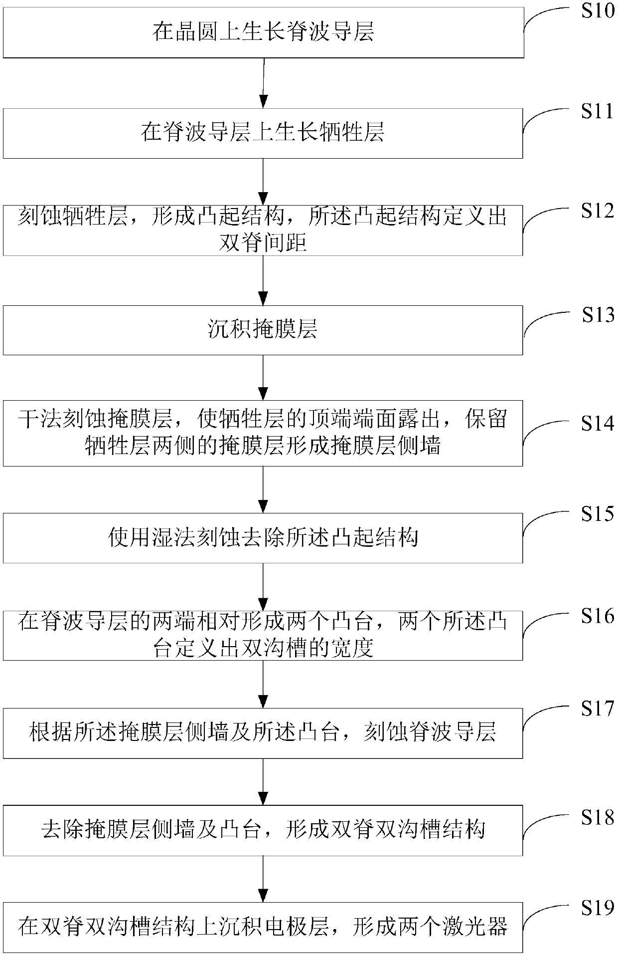
[0032] see figure 1 , the invention provides a kind of manufacturing method of laser chip, comprises steps:

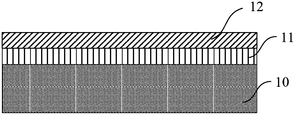
[0033] Please also see figure 2 , step S10 , growing a ridge waveguide layer 11 on the wafer 10 .

[0034] Ridge waveguide layer 11 is located on wafer 10 . Wafer 10 is suitable for various types of semiconductor lasers. Specifically, the ridge waveguide layer 11 generally includes a top layer and a bottom layer. The top layer is an InGaAs layer, and the bottom layer is an indium phosphide (InP) layer. Wherein, the thickness of the top laye...


PUM


Abstract

The invention provides a manufacture method of a laser chip. The manufacture method includes growing a ridge waveguide layer and a sacrificial layer; etching the sacrificial layer and forming a convexstructure which defines an inter-ridge distance; settling a mask layer; etching the mask layer so as to expose the top end face of the sacrificial layer and remaining the mask layer side walls on twosides of the sacrificial layer; removing the convex structure by adopting a wet etching method; defining the double groove position and the width; etching the ridge waveguide layer; removing the masklayer side walls through etching and forming a double-ridge double-groove structure; and settling an electrode layer. According to the invention, when testing laser chips manufactured by adopting theabove manufacture method, two lasers can be tested separately. Secondary picking can be performed in unqualified chips of the first picking, so that chip scrap is reduced, chip yield rate is improvedand chip manufacture cost is reduced.

Description

technical field [0001] The invention relates to the technical field of semiconductor optoelectronics, in particular to a manufacturing method of a laser chip. Background technique [0002] Distributed feedback lasers, DFB (Distributed Feedback) lasers, differ from Fabry-Perot lasers, FP (Fabry-Perot) lasers, in that DFB lasers have built-in Bragg gratings (BraggGrating), so the resonator of DFB lasers Has the ability to select modes. In the ideal case where the end face reflection is zero, there are two modes with the same and lowest resonator loss in the index-coupled DFB laser at a position symmetrical to the Bragg wavelength, that is, the index-coupled DFB laser is a dual-mode laser in principle of. However, at present, most DFB lasers are single-mode for practical DFB lasers. [0003] In the actual DFB laser, due to the reflection of the end faces at both ends of the grating, the reflectivity of the end faces at both ends of the grating is not zero, and the reflection...

Claims


Application Information

Patent Timeline
IPC IPC(8): H01S5/22H01S5/24
CPCH01S5/22H01S5/24
Inventor 尚飞方瑞禹
Owner HISENSE BROADBAND MULTIMEDIA TECH
Why Eureka
Try Eureka