Omnidirectional substrate integrated waveguide slot multi-antenna array

A substrate-integrated waveguide and slot antenna technology, applied in the field of communication technology applications, can solve the problems of large parasitic radiation with open circuit loss, complex feeding network, and limited gain of a single radiation unit, and achieve small circuit loss, isolation and anti-interference The effect of strong ability and simple structure

Inactive Publication Date: 2011-08-31
SOUTHEAST UNIV
View PDF3 Cites 7 Cited by
  • Summary
  • Abstract
  • Description
  • Claims
  • Application Information

AI Technical Summary

Problems solved by technology

[0004] As the frequency increases, the common open circuit has a large loss and serious parasitic radiation, and the common radiation oscillator, such as a dipole unit, has a limited gain of a single radiation unit. In order to increase the radiation gain, multiple radiation units need to be formed into an array, but The more radiating elements in the same array, the more complex the feeding network will be

Method used


Image

  • Omnidirectional substrate integrated waveguide slot multi-antenna array
  • Omnidirectional substrate integrated waveguide slot multi-antenna array
  • Omnidirectional substrate integrated waveguide slot multi-antenna array

Examples


Embodiment 1

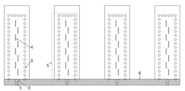
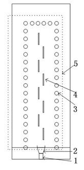
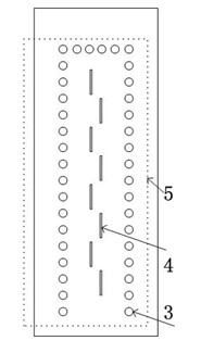
[0025] Example 1: figure 2 A schematic diagram of the metal structure on the upper surface of a single omnidirectional SIW slot antenna is given, image 3 A schematic diagram of the metal structure on the lower surface of a single omnidirectional SIW slot antenna is given. The substrate-integrated waveguide is composed of two rows of metallized through holes 3, and the 50-ohm microstrip feeder 1 and the SIW transmission line 5 are connected by a microstrip gradient line 2; the upper and lower surfaces of the substrate-integrated waveguide are engraved with slits 4 , the slits on the upper and lower surfaces are symmetrically distributed, and there are eight pairs in total; each slit has the same offset relative to the center line of the SIW, and the length and width of each slit are the same. image 3 The structural diagram of the omnidirectional SIW slot multi-antenna array is given. In order to keep the radiation pattern of a single antenna unchanged, an air gap is reserve...


PUM


Abstract

The invention relates to an omnidirectional substrate integrated waveguide slot multi-antenna array which comprises multiple omnidirectional substrate integrated waveguide slot antennas which are ranked side by side and integrally manufactured on a medium plate, wherein the space between the two adjacent omnidirectional substrate integrated waveguide slot antennas is at least the width of one single omnidirectional substrate integrated waveguide slot antenna; the omnidirectional substrate integrated waveguide slot antennas are two-sided symmetrical substrate integrated waveguide slot antennas; an upper surface metal layer is arranged on the front surface of the antenna, a lower surface metal layer is arranged on the back surface of the antenna, and a medium substrate (6) is arranged in the middle; metalized through holes (3) are symmetrically formed on the upper surface metal layer and the lower surface metal layer along the periphery of the antenna, thus the metalized through holes (3) enable the upper surface metal layer and the lower surface metal layer to be connected; slots (4) are alternately formed at the two sides of the central axis of the antenna; the metalized through holes (3) are not formed at one end of the central axis of the antenna, and the end is connected with a micro-strip transition line (2); and the other end of the micro-strip transition line (2) is connected with a feeder line (1).

Description

Technical field [0001] The invention is the field of communication technology, which involves a substrate integrated waveguide antenna array. [0002] Substrate Integrated Waveguide (SIW) gap an antenna, when using a dual -faced seamless gap, can form an omnidirectional radiation characteristics of the E surface, integrate multiple SIW gap an antenna unit on the same medium board to form multiple antenna array arraysAnd maintain a single antenna radiation direction diagram unchanged, belonging to the field of communication technology. Background technique [0003] In recent years, wireless communication technology has been developed rapidly and has been widely used.More and more communication systems require low cost, easy production, easy to integrate antennas integrated with other microwave RF plane circuits.High -frequency bands, omnidirectional radiation, easy production, and integrated antenna are one of the current research hotspots. At the same time, multi -antenna technol...

Claims


Application Information

Patent Timeline
Patent Type & Authority Applications(China)
IPC IPC(8): H01Q21/00H01Q1/38
Inventor 洪伟余晨周健义
Owner SOUTHEAST UNIV
Why Eureka
Try Eureka