Organic light-emitting diode display device and manufacturing method thereof

A light-emitting diode and display technology, which is applied in semiconductor/solid-state device manufacturing, semiconductor devices, electric solid-state devices, etc., can solve problems such as low production efficiency, long production process, and bad accumulation, so as to improve efficiency, reduce defect rate, and improve The effect of product yield

Active Publication Date: 2018-04-06
KUNSHAN GO VISIONOX OPTO ELECTRONICS CO LTD
View PDF3 Cites 8 Cited by
  • Summary
  • Abstract
  • Description
  • Claims
  • Application Information

AI Technical Summary

Problems solved by technology

[0005] The object of the present invention is to provide an organic light emitting diode display and its manufacturing method to solve the problems of long manufacturing process, easy accumulation of defects and low production efficiency in the existing manufacturing method

Method used


Image

  • Organic light-emitting diode display device and manufacturing method thereof
  • Organic light-emitting diode display device and manufacturing method thereof
  • Organic light-emitting diode display device and manufacturing method thereof

Examples


no. 1 example

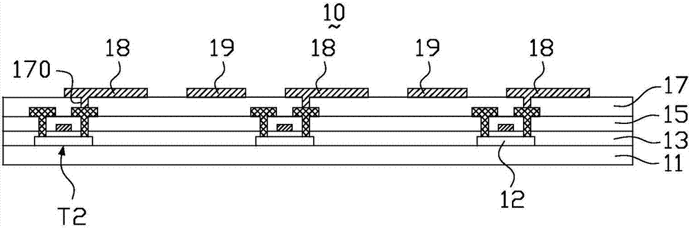
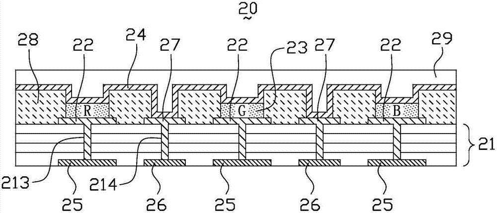
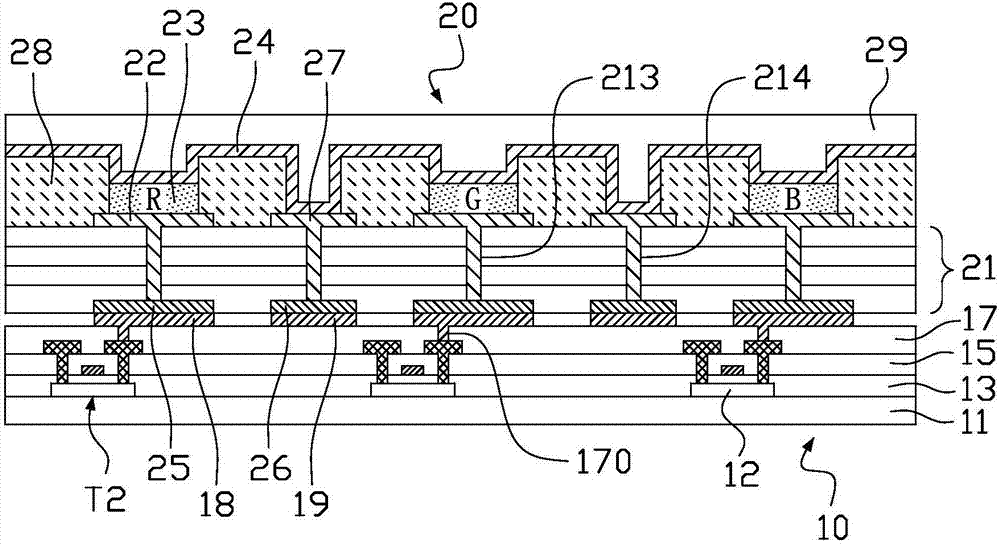
[0047] figure 1 is a schematic cross-sectional view of the array element substrate in the first embodiment of the present invention, figure 2 is a schematic cross-sectional view of the organic light emitting diode substrate in the first embodiment of the present invention, image 3 It is a schematic cross-sectional view of the organic light emitting diode display in the first embodiment of the present invention, please also refer to Figure 1 to Figure 3 , the organic light emitting diode display comprises an array element substrate 10 and an organic light emitting diode substrate 20, the array element substrate 10 and the organic light emitting diode substrate 20 are manufactured separately, and a thin film transistor array element (TFT) is formed on the array element substrate 10 An organic light emitting diode (OLED) is formed on the organic light emitting diode substrate 20, and then the two substrates 10, 20 are bonded together to form the organic light emitting diode d...

no. 2 example

[0080] Figure 10 is a schematic cross-sectional view of an organic light emitting diode display in a second embodiment of the present invention, Figure 11 is a schematic plan view of the array element substrate in the second embodiment of the present invention, Figure 12 It is a schematic front view of the organic light emitting diode substrate in the second embodiment of the present invention, Figure 13 It is a schematic diagram of the back of the organic light emitting diode substrate in the second embodiment of the present invention, please also refer to Figure 10 to Figure 13 , the structure and manufacturing method of the organic light emitting diode display in the second embodiment are basically the same as those in the first embodiment above, where the main difference is that the second bonding electrodes 19 on the array element substrate 10 are only distributed on the array element substrate 10 peripheral edge area and connected into a "mouth" shape (such as F...

no. 3 example

[0082] Figure 14 is a schematic cross-sectional view of an organic light emitting diode display in a third embodiment of the present invention, Figure 15 It is a schematic front view of the organic light emitting diode substrate in the third embodiment of the present invention, Figure 16It is a schematic diagram of the back of the organic light emitting diode substrate in the third embodiment of the present invention, please also refer to Figure 14 to Figure 16 , the structure and manufacturing method of the organic light emitting diode display in the third embodiment are basically the same as those in the first embodiment, the main difference is that the second bonding electrodes 19 on the array element substrate 10 are only distributed on the array element substrate 10 peripheral edge area and connected into a "mouth" shape (see Figure 11 shown), the fourth bonding electrode 26 and the fifth bonding electrode 27 are not provided on the organic light emitting diode sub...


PUM


Abstract

The invention provides an organic light-emitting diode display device and a manufacturing method thereof. The organic light-emitting diode display device is composed of an array element substrate andan organic light-emitting diode substrate that are oppositely bonded together. The array element substrate consists of a first substrate, a thin-film transistor array element arranged on the first substrate, and a first bonding electrode and a second bonding electrode, wherein the first bonding electrode and the second bonding electrode are arranged on the thin-film transistor array element. The organic light-emitting diode substrate includes a second substrate, a third bonding electrode arranged on a first surface of the second substrate, and an organic light-emitting diode arranged on an opposite second surface of the second substrate. On the basis of opposite bonding of the array element substrate and the organic light-emitting diode substrate, an LTPS preparation process and an OLED preparation process are carried out separately; and because the prepared flexible OLED substrate can be cut into any shape, one-time production of various products under a certain PPI is realized and thus utilization of multiple sets of evaporation masks is not needed, so that the cost is lowered and the production efficiency and the yield are improved.

Description

technical field [0001] The invention relates to the technical field of flat panel display, in particular to an organic light emitting diode display and a manufacturing method thereof. Background technique [0002] Organic Light-Emitting Diode (OLED) is an active light-emitting device, which has the advantages of high contrast, wide viewing angle, low power consumption, fast response, and thinner volume. It is expected to become the mainstream flat panel display technology of the next generation. [0003] Low temperature polysilicon thin film transistors (LTPS TFTs) have been commonly used on array substrates of flat panel displays such as active matrix organic light emitting diode displays (AMOLED). The manufacturing process of AMOLED displays is mainly divided into two parts: low-temperature polysilicon (LTPS) manufacturing and organic light-emitting diode (OLED) manufacturing. Specifically, the amorphous silicon layer (a-Si) is generally deposited on the substrate first, ...

Claims


Application Information

Patent Timeline
Patent Type & Authority Applications(China)
IPC IPC(8): H01L27/32H01L21/77
CPCH01L21/77H10K59/1275
Inventor 韩媛媛朱修剑
Owner KUNSHAN GO VISIONOX OPTO ELECTRONICS CO LTD
Why Eureka
Try Eureka