Circuit board processing method

A processing method and circuit board technology, applied in the directions of printed circuits, printed circuit manufacturing, electrical components, etc., can solve the problems of residual cutting powder, blockage of inner holes of substrates, and failure to remove cutting powder in time, so as to achieve convenient operation and prevent The inner hole is blocked and the drilling effect is better

Active Publication Date: 2018-04-06
重庆市志益鑫电子科技有限公司
View PDF5 Cites 0 Cited by
  • Summary
  • Abstract
  • Description
  • Claims
  • Application Information

AI Technical Summary

Problems solved by technology

[0004] At present, in the process of making circuit boards by drilling substrates, there are often bad situations where the inner holes of the substrates are blocked. One of the main reasons for this problem is that the cutting powder generated during drilling remains in the inner holes. That is, the cutting powder has not been removed in time

Method used


Image

  • Circuit board processing method

Examples


Embodiment Construction

[0023] Further detailed explanation through specific implementation mode below:

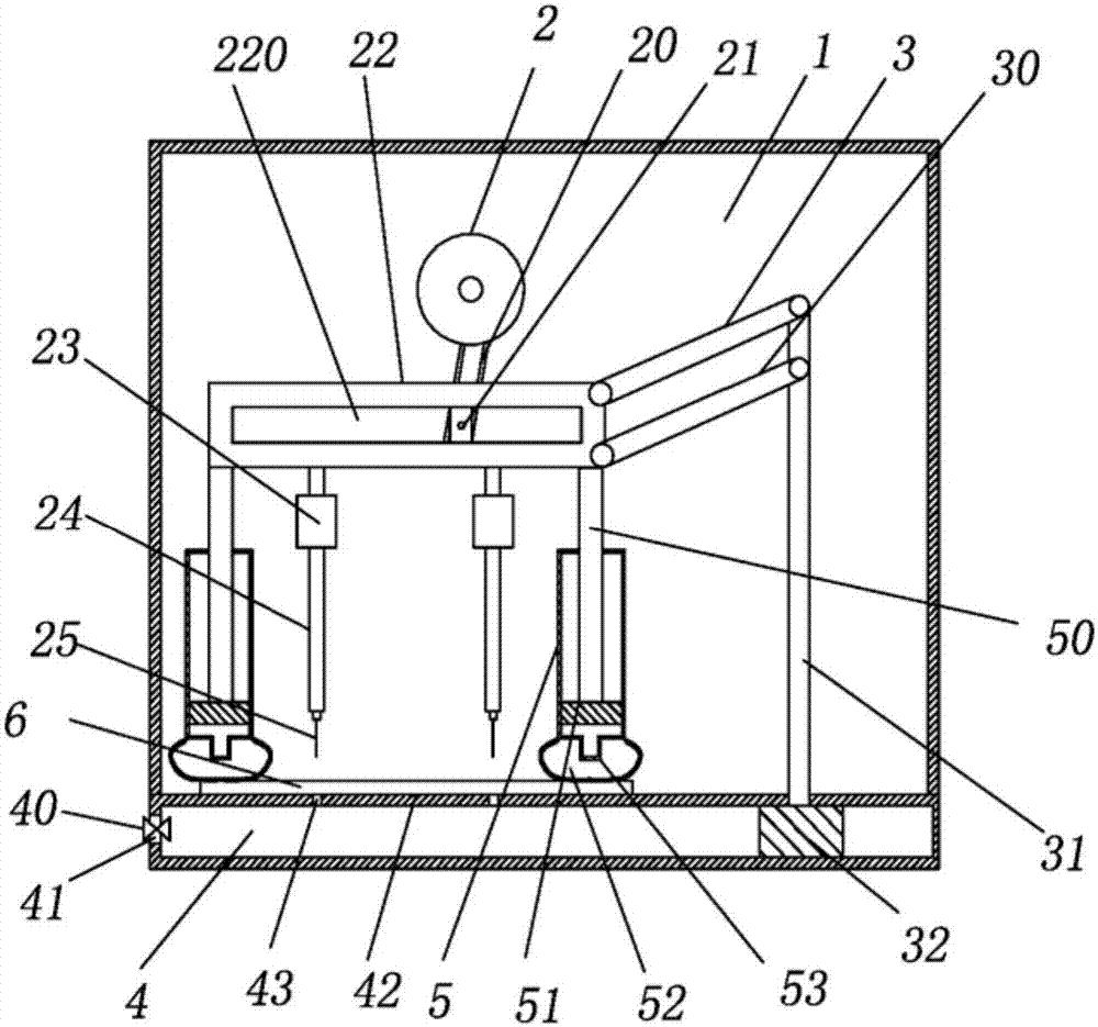
[0024] The reference signs in the accompanying drawings of the description include: frame 1, runner 2, extension rod 20, slider 21, moving frame 22, chute 220, support block 23, slide rod 24, drill bit 25, main swing rod 3, Auxiliary swing rod 30, straight rod 31, dust removal piston 32, dust removal chamber 4, air intake check valve 40, air inlet 41, support platform 42, punching hole 43, cylinder body 5, push-pull rod 50, air blowing piston 51, The airbag 52 , the gas injection port 53 , and the substrate 6 .

[0025] The embodiment is basically as attached figure 1 Shown: the circuit board processing method, comprises the following steps:

[0026] A. Cutting: Cut the large copper plate into several small copper plates;

[0027] B. Inner layer film: stick a dry film on the copper plate and expose it with ultraviolet rays;

[0028] C. Internal etching: put the exposed copper plate into the a...


PUM


Abstract

The invention belongs to the technical field of electronic device manufacturing, and particularly relates to a circuit board processing method. The circuit board processing method comprises the following steps of A, material opening, in which a large copper plate is cut into a plurality of small copper plates; B, inner-layer film formation, in which a dry film is attached onto the copper plate andis exposed by ultraviolet ray; C, internal etching; the exposed copper plate is placed in an alkali solution; D, brownization, composition and plate pressing to obtain a substrate; and E, drilling, in which a drilling device is arranged to drill, wherein the drilling device comprises a rack, a drilling mechanism and a dust removal mechanism, the drilling mechanism comprise a motor, a rotation wheel, a sliding block, a mobile rack, a support block, a sliding rod and a drilling head, and the dust removal mechanism comprises a main oscillating rod, a straight rod, a dust removal piston and a dust removal chamber. With the circuit board processing method disclosed by the technical scheme, cutting powder in holes in the substrate can be effectively removed, and inner hole plugging is prevented.

Description

technical field [0001] The invention belongs to the technical field of electronic device manufacturing, and in particular relates to a circuit board processing method. Background technique [0002] The circuit board (PCB) plays the role of the connection function in the entire electronic product, and when the function of the electronic product fails, the PCB is often the first to be suspected, and because the processing technology of the PCB is relatively complicated, so the PCB Production control is particularly strict and important. [0003] The production process of PCB is mainly divided into eight parts: inner layer circuit, lamination, drilling, hole metallization, outer layer dry film, outer layer circuit, silk screen, surface process and post process. The inner layer circuit specifically includes material cutting, inner layer film, inner etching, browning, typesetting, pressing plate, drilling and copper sinking. [0004] At present, in the process of making circuit...

Claims


Application Information

Patent Timeline
Patent Type & Authority Applications(China)
IPC IPC(8): H05K3/00
Inventor 胡红生
Owner 重庆市志益鑫电子科技有限公司
Why Eureka
Try Eureka