Automatic sample thinning method

A sample and defect technology, applied in the field of automated sample thinning, can solve the problems of low degree of automation, imprecise slicing position, high probability of sample preparation failure, low labor cost, high sample preparation success rate, and high degree of automation. Effect

Active Publication Date: 2018-04-10
SHANGHAI HUALI MICROELECTRONICS CORP
View PDF8 Cites 0 Cited by
  • Summary
  • Abstract
  • Description
  • Claims
  • Application Information

AI Technical Summary

Problems solved by technology

In the existing technology, it is necessary to manually observe the cutting position while slicing, the slicing position is very inaccurate, and the degree of automation is not high, the labor cost is high, and the efficiency is low
Moreover, it is not easy to cut the defect to the center, and the probability of sample preparation failure is high

Method used


Image

  • Automatic sample thinning method
  • Automatic sample thinning method
  • Automatic sample thinning method

Examples


Embodiment Construction

[0022] The present invention will be further described below with reference to the accompanying drawings and embodiments.

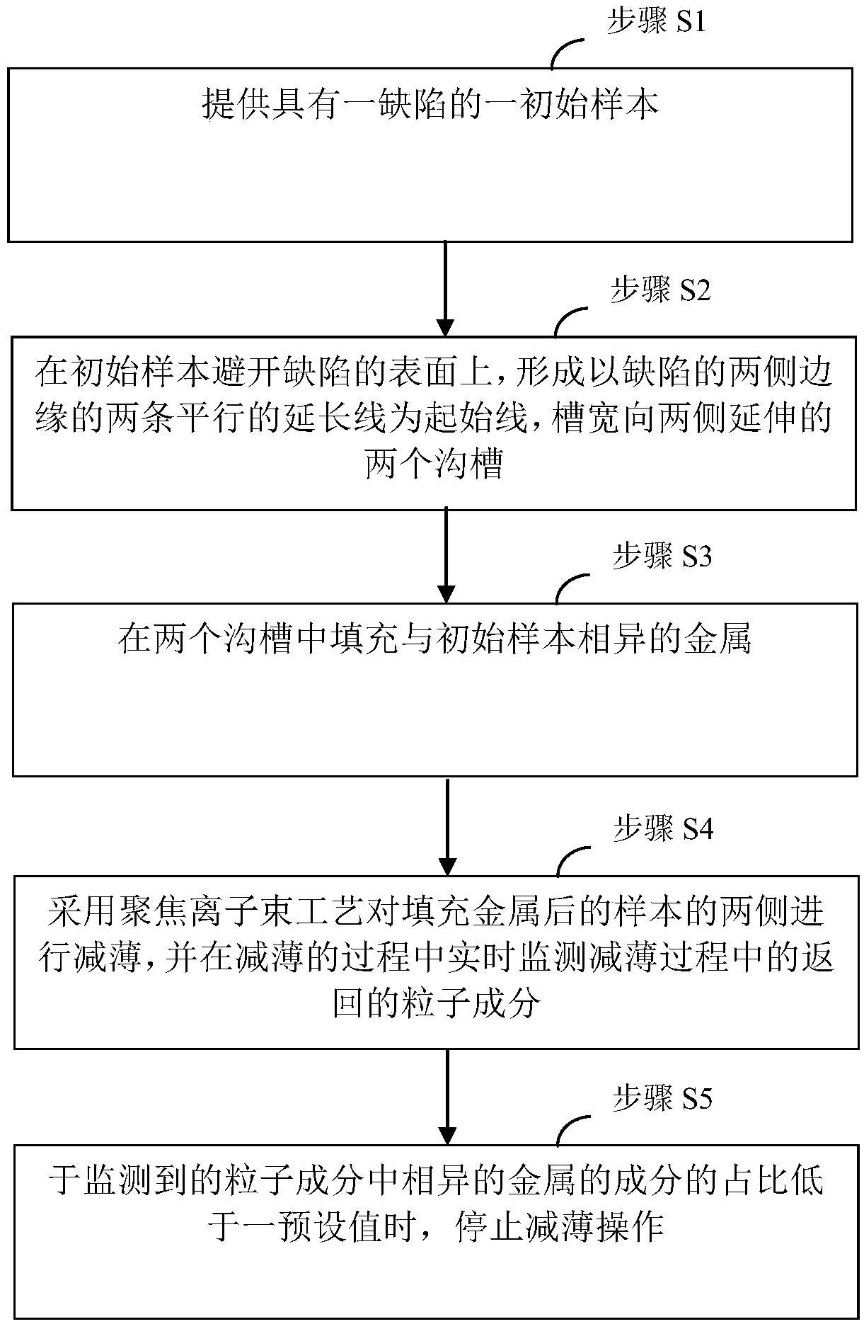
[0023] In a preferred embodiment, as figure 1 and figure 2 As shown, an automated sample thinning method is proposed, which is applied to prepare a failure analysis sample; which may include:

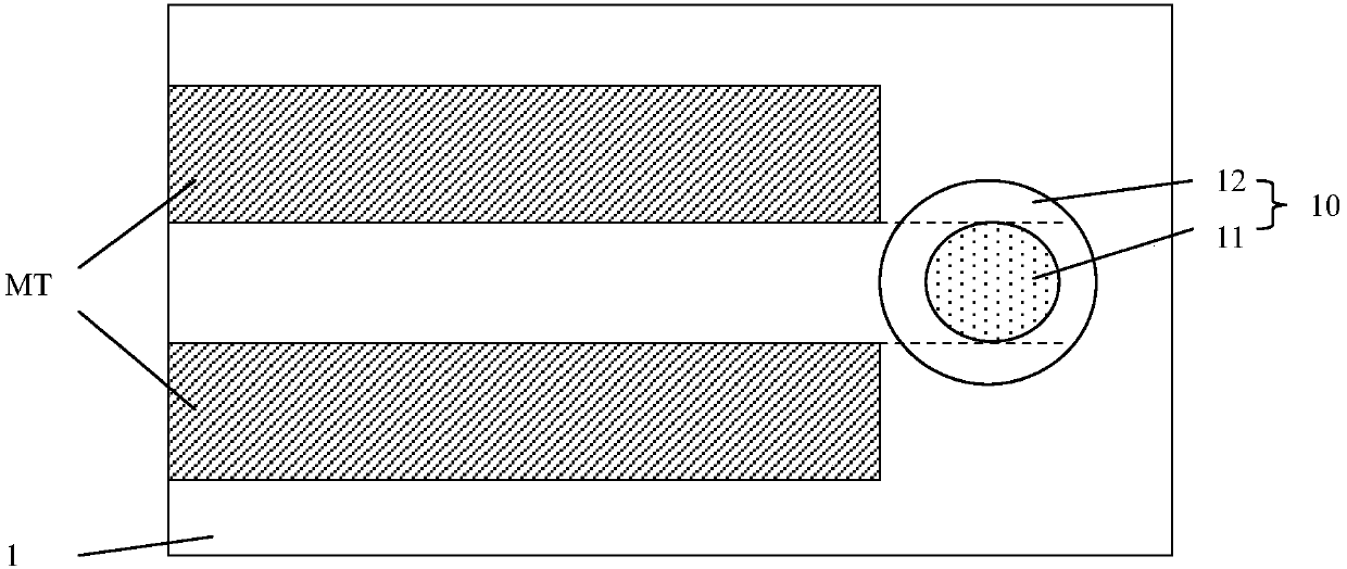
[0024] Step S1, providing an initial sample 1 with a defect 10;

[0025] Step S2, on the surface of the initial sample 1 avoiding the defect 10, forming two grooves with two parallel extension lines on both sides of the defect 10 as starting lines, and the groove width extending to both sides;

[0026] Step S3, filling the two trenches with metal MT different from the initial sample;

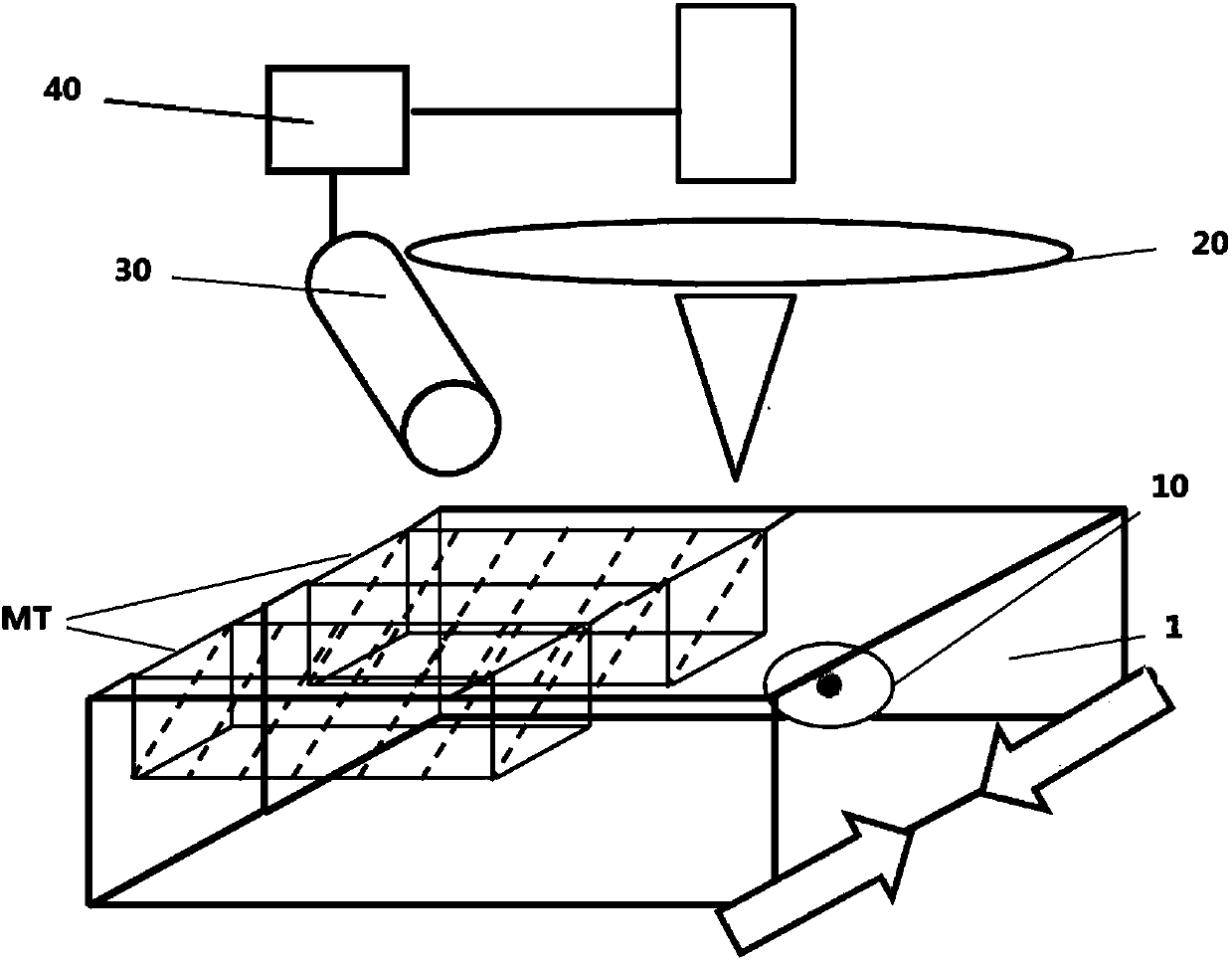
[0027] Step S4, using a focused ion beam process to thin both sides of the sample filled with the metal MT, and monitoring the returned particle composition in the thinning process in real time during the thinning process;

[0028] Step S5, when the proportion of the different m...


PUM


Abstract

The invention relates to the technical field of semiconductors, in particular to an automatic sample thinning method. The method includes the steps of S1, providing an initial sample with a defect; S2, forming two grooves in the surface, avoiding the defect, of the initial sample, wherein two parallel extension lines of the two lateral edges of the defect serve as the initial lines, and the groovewidth extends to the two sides; S3, filling the two grooves with metal different from the initial sample; S4, thinning the two sides of the sample filled with metal through a focused ion beam technology, and monitoring particle components returning in the thinning process in real time in the thinning process; S5, stopping the thinning operation when it is monitored that the ratio of the differentmetal components in the particle components is lower than a preset value. The position of focused ion cutting can be precisely controlled, slicing precision is improved, the automation degree is high, efficiency is high, labor cost is low, and the sample preparation success rate is high.

Description

technical field [0001] The present invention relates to the field of semiconductor technology, in particular to an automated sample thinning method. Background technique [0002] With the improvement of integrated circuit integration, the size of transistors in chips is getting smaller and smaller, and the minimum size of CD is also shrinking. The sensitivity of devices to tiny defects is gradually improved, and failure analysis methods face many challenges. [0003] Slicing using a focused ion beam defect inspection machine is a routine method for failure analysis. In the process of sample preparation, when encountering defects of small size, how to ensure that the core area can be cut is a major problem in the field. In the prior art, it is necessary to manually observe the cutting position while slicing, and the slicing position is very imprecise, and at the same time, the degree of automation is not high, the labor cost is high, and the efficiency is low. And it is not ...

Claims


Application Information

Patent Timeline
Patent Type & Authority Applications(China)
IPC IPC(8): G01N1/28
CPCG01N1/286G01N2001/2873
Inventor 周健刚曹秋凤龙吟王恺陈宏璘
Owner SHANGHAI HUALI MICROELECTRONICS CORP
Why Eureka
Try Eureka