Supercharge Your Innovation With Domain-Expert AI Agents!

Manufacturing method of tft substrate

A manufacturing method and substrate technology, applied in semiconductor/solid-state device manufacturing, semiconductor devices, electrical components, etc., can solve the problems of multiple photomask and photolithography processes, increase process time and process complexity, etc., to simplify the process and improve The effect of production efficiency

Active Publication Date: 2020-06-05
TCL CHINA STAR OPTOELECTRONICS TECH CO LTD
View PDF7 Cites 0 Cited by
  • Summary
  • Abstract
  • Description
  • Claims
  • Application Information

AI Technical Summary

Problems solved by technology

[0003] At present, the common structure of the oxide semiconductor thin film transistor (Thin Film Transistor, TFT) substrate is a structure with an etch stop layer (ESL), but this structure itself has certain problems, mainly manifested in the required photomask and photolithography process. Many, increasing the process time and process complexity

Method used


Image

  • Manufacturing method of tft substrate
  • Manufacturing method of tft substrate
  • Manufacturing method of tft substrate

Examples


Embodiment Construction

[0051] The following will clearly and completely describe the technical solutions in the embodiments of the present invention with reference to the accompanying drawings in the embodiments of the present invention. Obviously, the described embodiments are only part of the embodiments of the present invention, not all of them. Based on the embodiments of the present invention, all other embodiments obtained by persons of ordinary skill in the art without making creative efforts belong to the protection scope of the present invention.

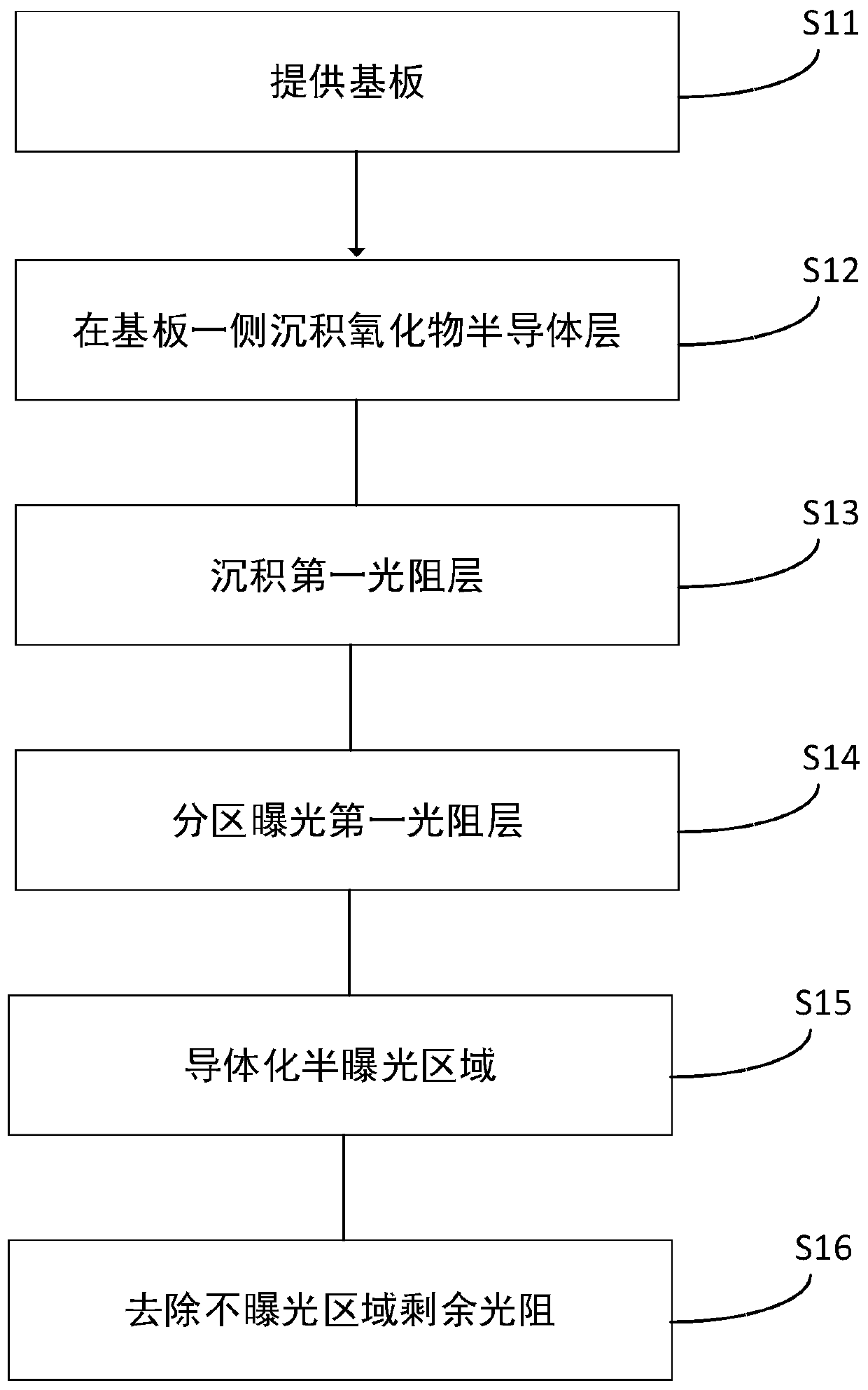
[0052] see figure 1 The manufacturing method flowchart of the TFT substrate 100, the manufacturing method of the first embodiment of the present invention specifically includes the following steps:

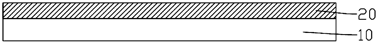
[0053] S11. providing the substrate 10;

[0054] Specifically, the substrate 10 may be a transparent substrate, such as glass, plastic and other materials.

[0055] S12. Depositing an oxide semiconductor layer 20 on one side of the substrate 10;

...


PUM


Abstract

The invention relates to the field of display manufacturing and a method for manufacturing a TFT substrate. Through the process of partition exposure, a semiconductor region is formed corresponding to the gate on the oxide semiconductor layer, a conductor region is formed corresponding to the region of the source electrode, the drain electrode and the pixel electrode, and the remaining part is removed to correspond to the position of the insulating region. Compared with the manufacturing method of the prior art, the TFT substrate that needs to be formed in four photolithography processes is compressed into three photolithography processes for molding, which saves one photolithography process flow, simplifies the process, and improves production efficiency.

Description

technical field [0001] The invention relates to the field of display technology, in particular to the manufacture of a TFT substrate. Background technique [0002] Organic Light Emitting Display (OLED) has self-illumination, no backlight, high contrast, thin thickness, wide viewing angle, fast response, can be used for flexible panels, and has a wide temperature range. It is considered to be an emerging application technology for the next generation of flat panel displays due to its excellent characteristics such as simple structure and manufacturing process. In the production of OLED large-size panels, oxide semiconductors have higher electron mobility, and compared with low-temperature polysilicon (LTPS), oxide semiconductors have a simpler process and higher compatibility with amorphous silicon processes, and are compatible with high-generation The production line is compatible and has been widely used. [0003] At present, the common structure of the oxide semiconducto...

Claims


Application Information

Patent Timeline
Patent Type & Authority Patents(China)
IPC IPC(8): H01L27/32H01L51/56
CPCH10K59/125
Inventor 韦显旺
Owner TCL CHINA STAR OPTOELECTRONICS TECH CO LTD
Features
  • R&D
  • Intellectual Property
  • Life Sciences
  • Materials
  • Tech Scout
  • Unparalleled Data Quality
  • Higher Quality Content
  • 60% Fewer Hallucinations
Learn More