A method for etching the base pedestal of a heterojunction bipolar transistor using a single-layer photomask
A heterojunction bipolar and transistor technology, applied in semiconductor devices, electrical components, circuits, etc., can solve the problems of wasted cost and disconnection of vapor-deposited gold wires, and achieve the effect of saving mask process, low cost, and simple realization.
- Summary
- Abstract
- Description
- Claims
- Application Information
AI Technical Summary
Problems solved by technology
Method used
Image
Examples
Embodiment Construction
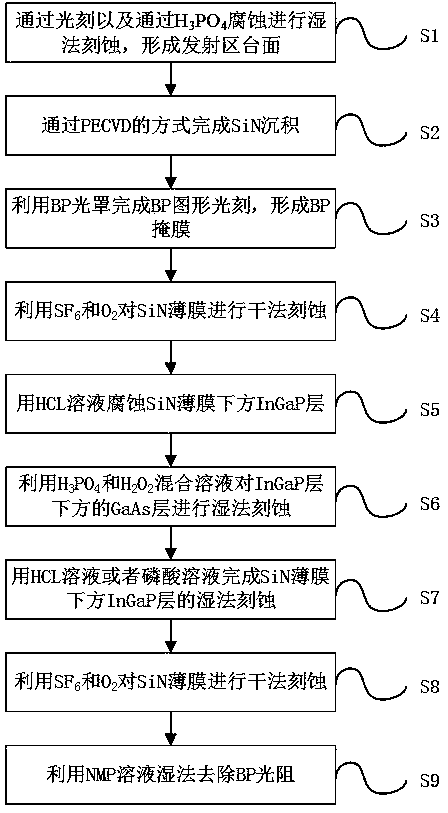
[0025] Describe technical scheme of the present invention in further detail below in conjunction with accompanying drawing: as figure 1 As shown, a heterojunction bipolar transistor base pedestal uses a single-layer photomask etching method, including the following steps:
[0026] S1: by photolithography and by H 3 PO 4 Etching is carried out by wet etching to form a mesa in the emission region and form an EM mesa made of GaAs material 1 such as figure 2 shown;
[0027] S2: SiN deposition is completed by PECVD, with a thickness of about 400 angstroms, which acts as a passivation layer, such as figure 2 SiN layer 2 shown in ;
[0028] S3: use the BP mask to complete the BP pattern photolithography to form a BP mask, such as figure 2 BP photoresist 5 shown;
[0029] S4: Utilize SF 6 and O 2 Dry etching of SiN films, such as image 3 shown;
[0030] S5: use HCL solution to etch the InGaP layer 3 under the SiN film, such as Figure 4 shown;
[0031] S6: Use H 3 PO ...
PUM
 Abstract
Description
Claims
Application Information
 - R&D Engineer
- R&D Manager
- IP Professional
- Industry Leading Data Capabilities
- Powerful AI technology
- Patent DNA Extraction
Browse by: Latest US Patents, China's latest patents, Technical Efficacy Thesaurus, Application Domain, Technology Topic, Popular Technical Reports.
© 2024 PatSnap. All rights reserved.Legal|Privacy policy|Modern Slavery Act Transparency Statement|Sitemap|About US| Contact US: help@patsnap.com


