Function test method and device of dsp module in fpga chip

A functional test and chip technology, applied in the field of FPGA chips, can solve problems affecting the data processing capability of FPGA chips and complex DSP module design, etc.

Active Publication Date: 2020-03-31
SHENZHEN PANGO MICROSYST CO LTD
View PDF7 Cites 0 Cited by
  • Summary
  • Abstract
  • Description
  • Claims
  • Application Information

AI Technical Summary

Problems solved by technology

[0003] However, while the ability of DSP to process data in the FPGA chip is getting stronger and stronger, the design of the DSP module in the FPGA chip is also becoming more and more complicated. The correctness of the function of the DSP module in the FPGA chip after tape-out will directly affect the performance of the FPGA chip. Therefore, how to quickly complete the functional test of all DSP modules in each FPGA chip under limited test conditions is particularly important. It is related to whether the rapid screening of FPGA chips can be completed and the performance of FPGA chips can be improved. Productivity

Method used


Image

  • Function test method and device of dsp module in fpga chip
  • Function test method and device of dsp module in fpga chip
  • Function test method and device of dsp module in fpga chip

Examples


Embodiment 1

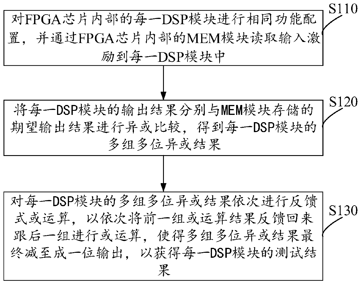
[0027] Such as figure 1 As shown, embodiment one of the present invention proposes a kind of function test method of DSP module in FPGA chip, and this function test method comprises the following steps:

[0028] Step S110: Perform the same functional configuration on each DSP module inside the FPGA chip, and read input and stimulate each DSP module through the MEM module inside the FPGA chip.

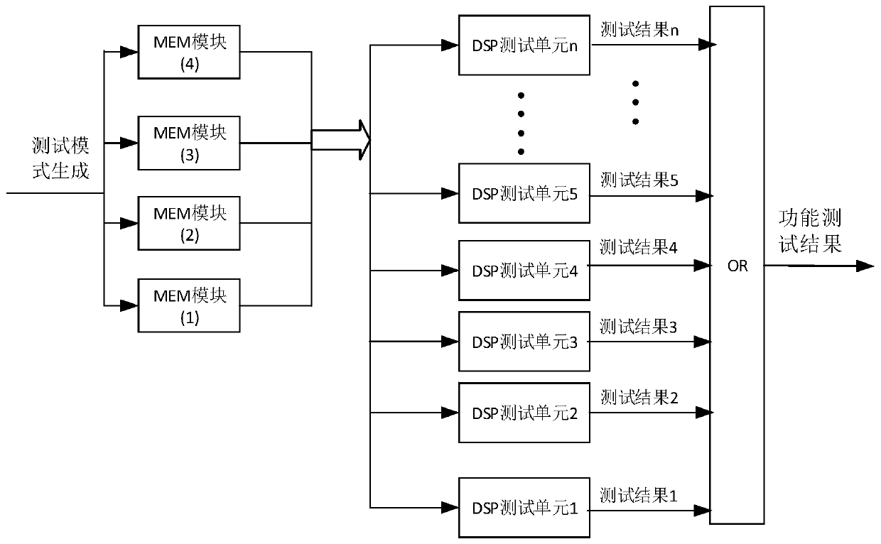
[0029] Specifically, when we want to perform a functional test on all the DSP modules in the FPGA chip, we need to perform the same functional configuration on each DSP module so as to perform the corresponding functional test. At the same time, due to the programmable features inside the FPGA chip, we can connect the corresponding inputs of all DSP modules in the FPGA chip to the outputs of the MEM modules through the wiring resources inside the FPGA chip, that is, as figure 2 shown. In this way, when we perform a functional test on the DSP module in the FPGA chip, we only need one ...

Embodiment 2

[0044] Such as Figure 4 As shown, embodiment two of the present invention proposes a kind of functional testing method of DSP module in FPGA chip, and this functional testing method comprises the following steps:

[0045] Step S210: Perform the same functional configuration on each DSP module inside the FPGA chip, and read the input stimulus to each DSP module through the MEM module inside the FPGA chip.

[0046] Specifically, when we want to perform a functional test on all the DSP modules in the FPGA chip, we need to perform the same functional configuration on each DSP module so as to perform the corresponding functional test. At the same time, due to the programmable features inside the FPGA chip, we can connect the corresponding inputs of all DSP modules in the FPGA chip to the outputs of the MEM modules through the wiring resources inside the FPGA chip, that is, as figure 2 shown. In this way, when we perform a functional test on the DSP module in the FPGA chip, we o...

Embodiment 3

[0063] Such as Figure 5 As shown, embodiment two of the present invention proposes a kind of functional testing method of DSP module in FPGA chip, and this functional testing method comprises the following steps:

[0064] Step S310: Perform the same functional configuration on each DSP module inside the FPGA chip, and read input and stimulate each DSP module through the MEM module inside the FPGA chip.

[0065] Specifically, when we want to perform a functional test on all the DSP modules in the FPGA chip, we need to perform the same functional configuration on each DSP module so as to perform the corresponding functional test. At the same time, due to the programmable features inside the FPGA chip, we can connect the corresponding inputs of all DSP modules in the FPGA chip to the outputs of the MEM modules through the wiring resources inside the FPGA chip, that is, as figure 2 shown. In this way, when we perform a functional test on the DSP module in the FPGA chip, we onl...


PUM


Abstract

The invention discloses a function test method and a function test device of a DSP module in an FPGA chip, and belongs to the field of FPGA chip technology. The function test method includes the stepsof performing the same function configuration on each DSP module inside an FPGA chip, and reading an input excitation into each DSP module through an MEM module inside the FPGA chip; conducting an XOR comparison between an output result of each DSP module with an expected output result stored in the MEM module to obtain multiple sets of multi-bit XOR results of each DSP module; and performing feedback OR operation on the multiple sets of multi-bit XOR results of each DSP module in sequence to feed back a previous set of OR operation results back sequentially to undergo OR operation with the following set, so that the multiple sets of multi-bit XOR results are finally reduced to one bit output to obtain a test result of each DSP module. According to the invention, the requirement on test conditions can be minimized, and the function test on all the DSP modules in the FPGA chip can be completed simply by means of the MEM module in the FPGA chip.

Description

technical field [0001] The invention relates to the technical field of FPGA chips, in particular to a function testing method and a function testing device of a DSP module in an FPGA chip. Background technique [0002] With the rapid development of integrated circuits, FPGA (Field-Programmable Gate Array, Field Programmable Gate Array) chip, as a programmable logic device, has gradually evolved from a peripheral device of electronic design to a digital system in just over 20 years. With the advancement of semiconductor process technology, the design technology of FPGA chips has achieved leap-forward development and breakthroughs, achieving the characteristics of high density, high security, low power consumption, low cost, system integration, and dynamic reconfigurability. Chips have been widely used in communications, aerospace, consumer electronics and other fields. In recent years, with the rapid development of some data processing services such as information technology...

Claims


Application Information

Patent Timeline
Patent Type & Authority Patents(China)
IPC IPC(8): G01R31/317G01R31/3181
CPCG01R31/31703G01R31/3181
Inventor 蒯金周忠斌
Owner SHENZHEN PANGO MICROSYST CO LTD
Why Eureka
Try Eureka