
Silicon-based fan-out package of integrated heat-dissipation structure and wafer-level packaging method

A wafer-level packaging, integrated heat dissipation technology, applied in electrical components, electric solid state devices, circuits, etc., can solve the problems of low chip heat dissipation efficiency, complex integrated manufacturing, and high manufacturing cost, and achieve light weight, high integration density, and price. low effect

Pending Publication Date: 2018-04-20
HUATIAN TECH KUNSHAN ELECTRONICS
View PDF0 Cites 12 Cited by
  • Summary
  • Abstract
  • Description
  • Claims
  • Application Information

AI Technical Summary

Problems solved by technology

However, plastic encapsulation materials generally have poor thermal conductivity, which makes the heat dissipation efficiency of the chip lower, requiring an additional integrated heat dissipation structure, but the integration of the additional heat dissipation structure is more complicated and the production cost is high

Method used


Image

  • Silicon-based fan-out package of integrated heat-dissipation structure and wafer-level packaging method
  • Silicon-based fan-out package of integrated heat-dissipation structure and wafer-level packaging method
  • Silicon-based fan-out package of integrated heat-dissipation structure and wafer-level packaging method

Examples


Embodiment Construction

[0030] In order to understand the technical content of the present invention more clearly, the following examples are given in detail, the purpose of which is only to better understand the content of the present invention but not to limit the protection scope of the present invention. The components in the structures in the drawings of the embodiments are not scaled according to the normal scale, so they do not represent the actual relative sizes of the structures in the embodiments.

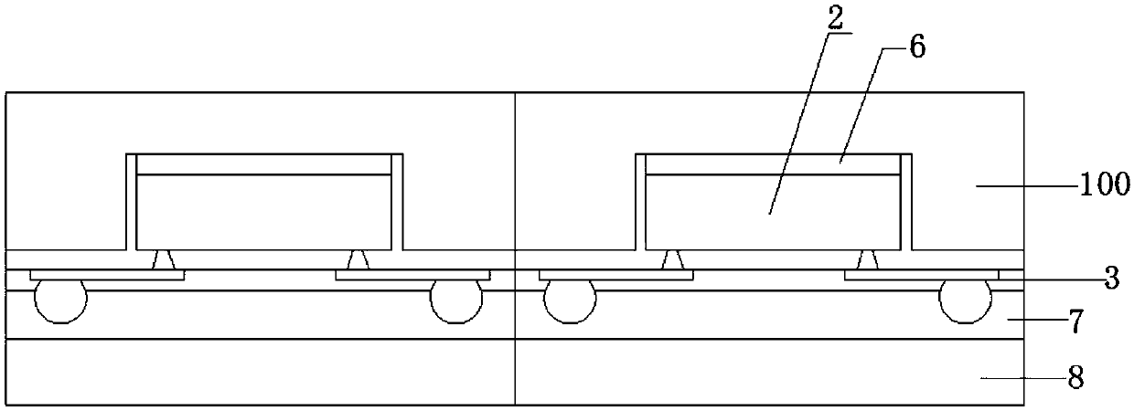
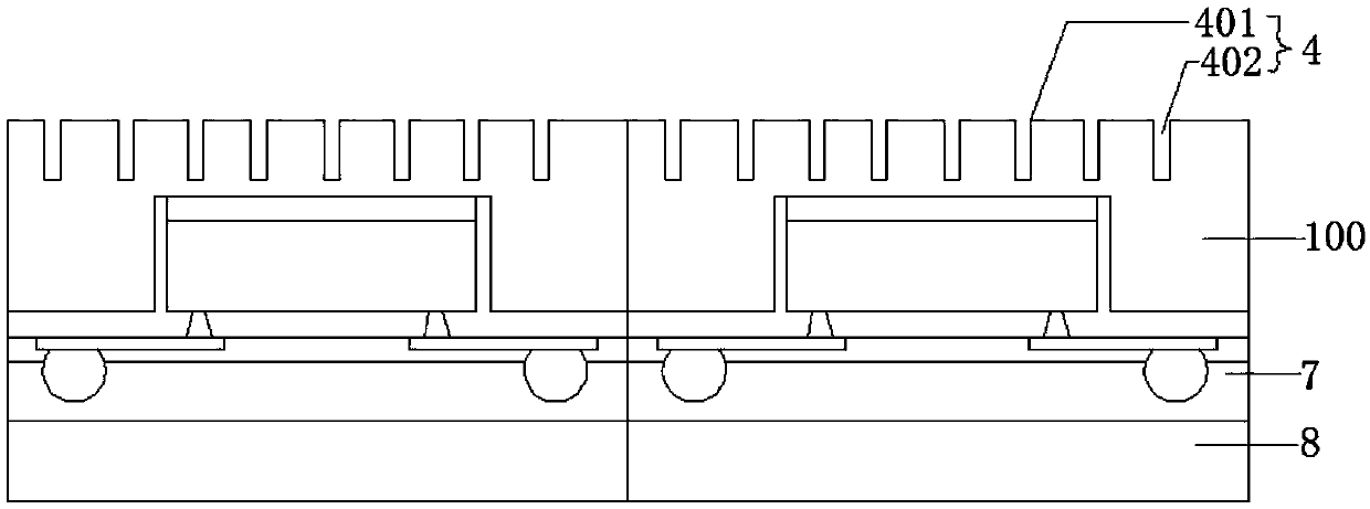
[0031] Such as Figure 5 As shown, a silicon-based fan-out package with an integrated heat dissipation structure includes a silicon substrate 1, the silicon substrate has a first surface 101 and a second surface 102, and at least one direction is formed on the first surface of the silicon substrate. The groove 103 extending on the second surface is provided with at least one chip 2 with the pad facing upward in the groove, the pad surface of the chip has a pad, and the electricity of at least on...


PUM


Abstract

The invention discloses a silicon-based fan-out package of an integrated heat-dissipation structure and a wafer-level packaging method. Based on a silicon-based fan-out package technology, a heat-dissipation structure is directly formed on a second surface of a silicon substrate after a chip is embedded. A wafer-level process is used for manufacturing, the machining is high-precision, the processis simple, and the price is low. Compared with conventional mechanically processed heat sinks, the silicon-based fan-out package can use a silicon micromachining process directly on a silicon substrate to produce a finer heat dissipation structure, create a larger heat dissipation area within the same unit volume, and achieve better heat radiation. This heat dissipation structure is directly integrated on the backside of a chip embedded in a silicon substrate, and has a high integration density, a small size, and a light weight. In addition, the interface between the external environment and the chip is reduced, and the heat dissipation effect is further improved. Preferably, a heat-dissipating cover plate with forced water cooling can be integrated on the heat dissipation structure of thesecond surface of the silicon substrate to obtain better heat dissipation efficiency.

Description

technical field [0001] The invention relates to the technical field of semiconductor packaging, in particular to a silicon-based fan-out packaging with an integrated heat dissipation structure and a wafer-level packaging method. Background technique [0002] Wafer-level fan-out packaging refers to reconfiguring the wafer and wafer-level rewiring method, and the I / O is covered with the rewiring surface array to cover the packaging surface, so as to expand the I / O pitch and meet the requirements of the next level of interconnection. pitch requirements. [0003] At present, in the traditional fan-out packaging technology typically represented by eWLB, the five sides of the chip are wrapped with an epoxy molding compound. However, plastic encapsulation materials generally have poor thermal conductivity, so that the heat dissipation efficiency of the chip is low, and an additional integrated heat dissipation structure is required, but the integration of the additional heat dissi...

Claims


Application Information

Patent Timeline
IPC IPC(8): H01L23/29H01L23/31H01L23/367
CPCH01L23/298H01L23/31H01L23/367H01L2224/73267H01L2224/97H01L2924/15153H01L2924/15159H01L2224/04105H01L2224/12105H01L2224/83
Inventor 王腾
Owner HUATIAN TECH KUNSHAN ELECTRONICS
Learn More