A chip structure and manufacturing method

A technology of chip structure and manufacturing method, which is applied in semiconductor/solid-state device manufacturing, semiconductor/solid-state device components, semiconductor devices, etc., can solve problems such as signal crosstalk, and achieve the effects of improving performance, cost advantages, and high production efficiency

Active Publication Date: 2020-03-06
NAT CENT FOR ADVANCED PACKAGING CO LTD
View PDF5 Cites 0 Cited by
  • Summary
  • Abstract
  • Description
  • Claims
  • Application Information

AI Technical Summary

Problems solved by technology

[0005] Therefore, the technical problem to be solved by the present invention is to overcome the defect that the packaging structure in the prior art is prone to signal crosstalk, thereby providing a chip structure and manufacturing method

Method used


Image

  • A chip structure and manufacturing method
  • A chip structure and manufacturing method
  • A chip structure and manufacturing method

Examples


Embodiment 1

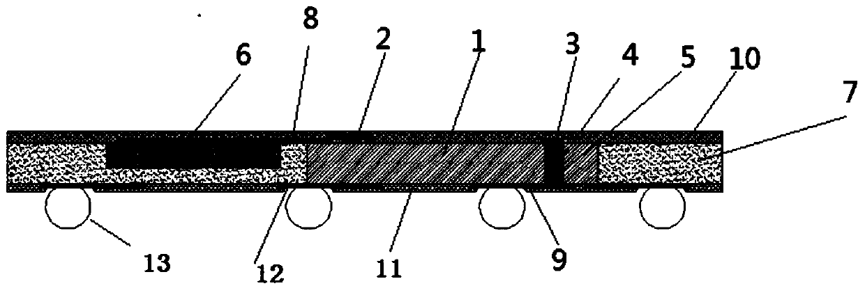
[0052] An embodiment of the present invention provides a chip structure, such as figure 1 shown, including:

[0053] The chip substrate 1 is provided with a first signal pad 2 and a second signal pad 3 on the first surface of the chip substrate 1, and on the second surface of the chip substrate 1, the position corresponding to the second signal pad 3 is engraved A first hole 4 is etched through the chip substrate 1, and the first hole 4 is filled with a metal conductive material 5; a dielectric material 6 is arranged at a preset distance from the chip substrate 1; an encapsulation material 7 is partially wrapped around the chip substrate 1 and dielectric material 6, the packaging material 7 is exposed on the same side of the dielectric material 6 and the first signal pad 1 and the second signal pad 2, and the first signal line is arranged on the packaging material 7 and the second signal pad 3 8; the second signal line 9 is laid on different sides of the packaging material 7 ...

Embodiment 2

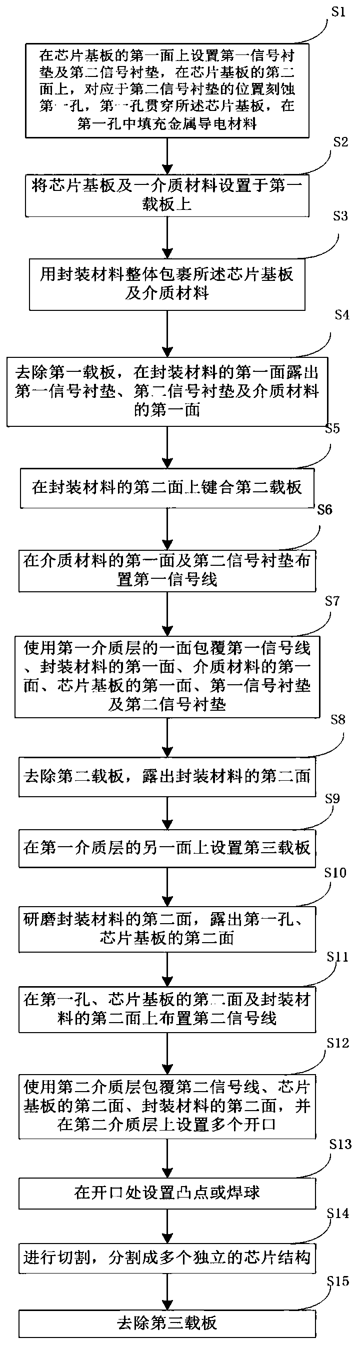
[0059] An embodiment of the present invention provides a method for manufacturing a chip structure, such as figure 2 shown, including the following steps:

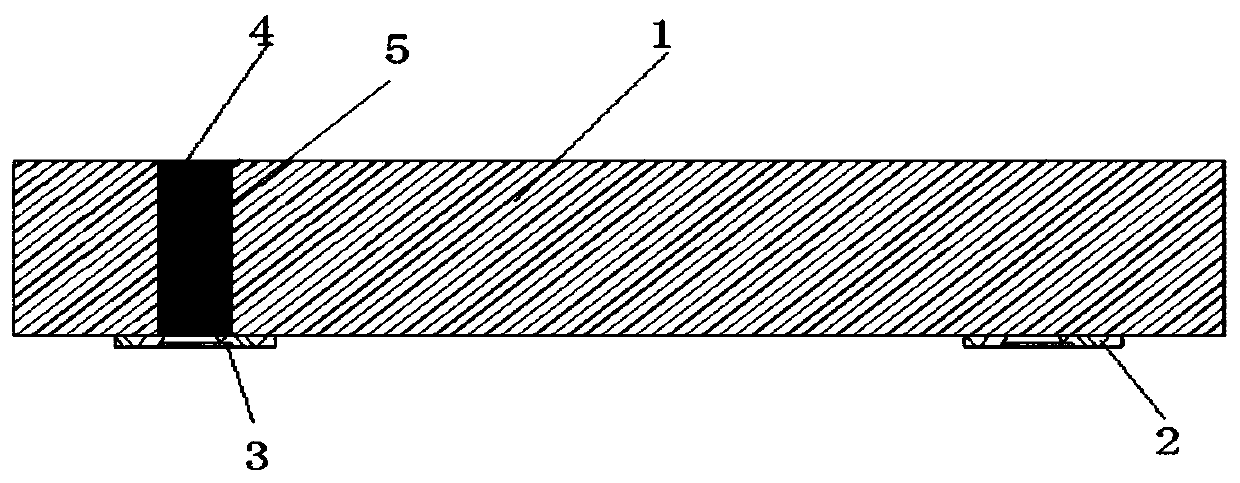
[0060] Step S1: if image 3 As shown, the first signal pad 2 and the second signal pad 3 are arranged on the first surface of the chip substrate 1, and the second signal pad 3 is etched on the second surface of the chip substrate 1 corresponding to the position of the second signal pad 3. A hole 4 , the first hole 4 runs through the chip substrate 1 , and the first hole 4 is filled with metal conductive material 5 . In the embodiment of the present invention, the first signal pad 2 is a low-frequency signal PAD, the second signal pad 3 is a high-frequency signal PAD, and the conductive metal material 5 can be, for example, copper.

[0061] Step S2: if Figure 4 As shown, the chip substrate 1 and a dielectric material 6 are disposed on the first carrier 21 . In practical applications, different dielectric materials 6 c...


PUM


Abstract

The invention discloses a chip structure and a manufacturing method. The chip structure comprises a chip substrate, a first signal gasket, a second signal gasket, a first hole, a dielectric material and a packaging material, wherein a first surface of the chip substrate is provided with the first signal gasket and the second signal gasket; on a second surface of the chip substrate, the first holeis etched at a position corresponding to the second signal gasket; the first hole passes through the chip substrate and a metal conductive material is filled in the first hole; the dielectric materialand the chip substrate are arranged at a preset distance interval; a part of the packaging material wraps the chip substrate and the dielectric material, the packaging material is exposed at a side of the dielectric material, the side of the dielectric material is the same with the sides of the first signal gasket and the second signal gasket, and a first signal line is arranged on the packagingmaterial and the second signal gasket; and the side of the packaging material, which is different from the sides of the first signal gasket and the second signal gasket, is provided with a second signal line. In the invention, based on double-sided wiring of a silicon through hole, wiring difficulty of packaging is reduced, simultaneously high frequency and low frequency signals are separated so that crosstalk among the signals is reduced.

Description

technical field [0001] The invention relates to the field of semiconductor packaging, in particular to a chip structure and a manufacturing method. Background technique [0002] With the trend of multi-function and miniaturization of electronic products, high-density microelectronic assembly technology has gradually become the mainstream in the new generation of electronic products. In order to cope with the development of a new generation of electronic products, especially the development of smart phones, PDAs, ultrabooks and other products, the size of chips is developing in the direction of higher density, faster speed, smaller size, and lower cost. The emergence of fan-out wafer level packaging technology (Fanout Panel Level Package, F0PLP), as an upgrade technology of fan-out wafer level packaging technology (Fanout Wafer Level Package, F0WLP), has a broader development prospect. [0003] In high-frequency electronic equipment, a section of copper skin with a special s...

Claims


Application Information

Patent Timeline
Patent Type & Authority Patents(China)
IPC IPC(8): H01L23/48H01L21/768H01L23/485H01L21/60
CPCH01L21/76898H01L23/481H01L2224/0231H01L2224/02333H01L2224/02381H01L2224/18
Inventor 徐健
Owner NAT CENT FOR ADVANCED PACKAGING CO LTD
Why Eureka
Try Eureka