Color film substrate and preparation method thereof, and display device

一种彩膜基板、彩膜层的技术,应用在彩膜基板及其制备方法以及显示装置领域,能够解决彩膜基板良率低等问题,达到良率高、易于实现、简化工艺的效果

Active Publication Date: 2018-04-20
BOE TECH GRP CO LTD
View PDF7 Cites 4 Cited by
  • Summary
  • Abstract
  • Description
  • Claims
  • Application Information

AI Technical Summary

Problems solved by technology

Therefore, the preparation of large-size, high-definition display devices in the future needs to focus on research on top-emission active-driven organic light-emitting devices (AM-OLEDs), which require OLED devices to be used in conjunction with thin-film transistors (TFTs), but due to the poor quality of current color filter substrates The low efficiency cannot meet the requirements of use, resulting in many process problems in the process of laminating the TFT array substrate and the color filter substrate

Method used


Image

  • Color film substrate and preparation method thereof, and display device
  • Color film substrate and preparation method thereof, and display device
  • Color film substrate and preparation method thereof, and display device

Examples


Embodiment 1

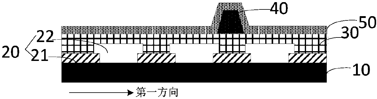
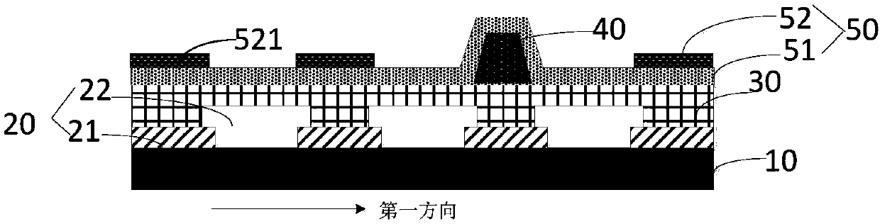
[0068] In this example, refer to Figure 6 to Figure 9 and figure 2 , wherein the electrode 50 includes a transparent conductive oxide electrode 51 and sub-metal electrodes 521 arranged at intervals in the first direction, and the method for preparing the color filter substrate is as follows:

[0069] 1. The glass substrate 10 is cleaned, and the black matrix 21, the color filter 22, and the cover layer 30 are continuously deposited on the substrate 10, wherein the color filters 22 are deposited successively during the preparation of the R, G, and B color filters, And make the color filter 22 have a certain coverage to the black matrix 21;

[0070] 2. Deposit the spacer 40 material and form a pattern, so that the spacer 40 pattern is located directly above the light-shielding metal pattern (or black matrix 21 pattern), and the width of the pattern is slightly smaller than the width of the black matrix 21 pattern;

[0071] 3. Deposit a layer of transparent conductive oxide e...

Embodiment 2

[0074] In this example, refer to Figure 6 to Figure 9 and image 3 , wherein the electrode 50 includes a transparent conductive oxide electrode 51 and a first transparent metal surface electrode 522, and the method for preparing the color filter substrate is as follows:

[0075] 1. The glass substrate 10 is cleaned, and the black matrix 21, the color filter 22, and the covering layer 30 are continuously deposited on the substrate 10, and the color filters of R, G, and B are successively deposited during the preparation of the color filter 22 , and make the color filter 22 cover the black matrix 21 to a certain extent;

[0076] 2. Deposit 40 layers of spacer material and form a pattern, so that the spacer 40 pattern is located directly above the black matrix 21 pattern, and the width of the pattern is slightly smaller than the width of the black matrix 21 pattern;

[0077] 3. Finally deposit a layer of transparent conductive oxide electrode 51 film and a thin layer of transp...

Embodiment 3

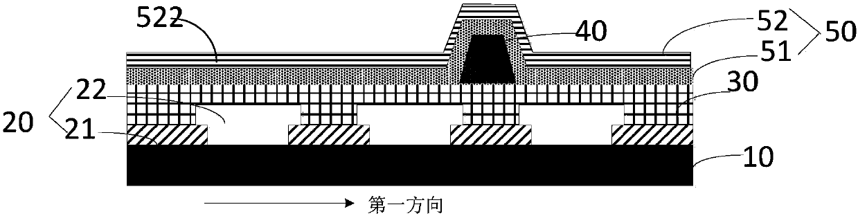
[0079] In this example, refer to Figure 6 to Figure 9 and Figure 4 , wherein the electrode 50 includes a second transparent metal surface electrode 523, and the method for preparing the color filter substrate is as follows:

[0080] 1. The glass substrate 10 is cleaned, and the black matrix 21, the color filter 22, and the covering layer 30 are continuously deposited on the substrate, and the color filters of R, G, and B are successively deposited during the preparation of the color filter 22 layers, And make the color filter 22 have a certain coverage to the black matrix 21;

[0081] 2. Deposit 40 layers of spacer material and form a pattern, so that the spacer 40 pattern is located directly above the black matrix 22 pattern, and the width of the pattern is slightly smaller than the width of the black matrix 22 pattern;

[0082] 3. Finally, a thin layer of transparent metal electrode 523 is deposited, and its material can be Ag, Al, Mg, Ca, Sm, etc., or alloys thereof suc...


PUM


Abstract

The present invention provides a color film substrate and a preparation method thereof, and a display device. The color film substrate comprises: a substrate; a color film layer arranged on a first surface of the substrate and comprising a black matrix and color filters which are arranged in the same layer; a covering layer arranged on a surface, far away from the substrate, of the color film layer; a spacer arranged on a surface, far away from the substrate, of the covering layer; and an electrode arranged on a surface, far away from the substrate, of the covering layer, wherein the spacer iscovered with the electrode. The inventor discovers that: the spacer directly arranged on the surface of the covering layer has high anchoring strength to allow the spacer to be firmly attached to thesurface of the covering layer and not to be easily fell off, and therefore, the product yield rate is improved, the electrode is good in conductive performance and can effectively protect the spaces,the color film substrate is simple in structure, easy to realize and low in cost.

Description

technical field [0001] The present invention relates to the field of display technology, in particular, to a color filter substrate, a preparation method thereof, and a display device. Background technique [0002] Currently, OLED display devices are receiving more and more attention due to their excellent performance. Among them, according to the different directions in which light is emitted from the OLED device in the display, it is mainly divided into two different structures: one is a bottom-emitting OLED device, and the other is a top-emitting OLED device. In the bottom-emitting device, the light can only be partially emitted from the openings provided on the array substrate, and most of the light is wasted, and the aperture ratio is low, and the aperture ratio will decrease as the definition increases; In the emitting device, the light emitted from the top of the device is not affected by the thin film transistor (TFT) in the array substrate, so the aperture ratio ca...

Claims


Application Information

Patent Timeline
Patent Type & Authority Applications(China)
IPC IPC(8): H01L27/32
CPCH10K59/38H10K59/12H10K59/1315H10K50/814H10K50/816H10K50/824H10K50/8428H10K50/865H10K2102/3026H10K50/828H10K59/126H10K71/00
Inventor 王国英宋振
Owner BOE TECH GRP CO LTD
Why Eureka
Try Eureka