
DFB laser and manufacturing method thereof

A technology of DFB lasers and manufacturing methods, which is applied in the field of lasers, can solve problems and cannot meet the needs of use, and achieve the effect of easy reflection

Inactive Publication Date: 2018-04-20
WUHAN TELECOMM DEVICES
View PDF3 Cites 5 Cited by
  • Summary
  • Abstract
  • Description
  • Claims
  • Application Information

AI Technical Summary

Problems solved by technology

In general, the optical power can be increased by increasing the cavity length and current injection, but there will be problems with the SMSR output spectrum at high or low temperatures, and it cannot meet the needs of use.

Method used


Image

  • DFB laser and manufacturing method thereof
  • DFB laser and manufacturing method thereof
  • DFB laser and manufacturing method thereof

Examples


Embodiment 1

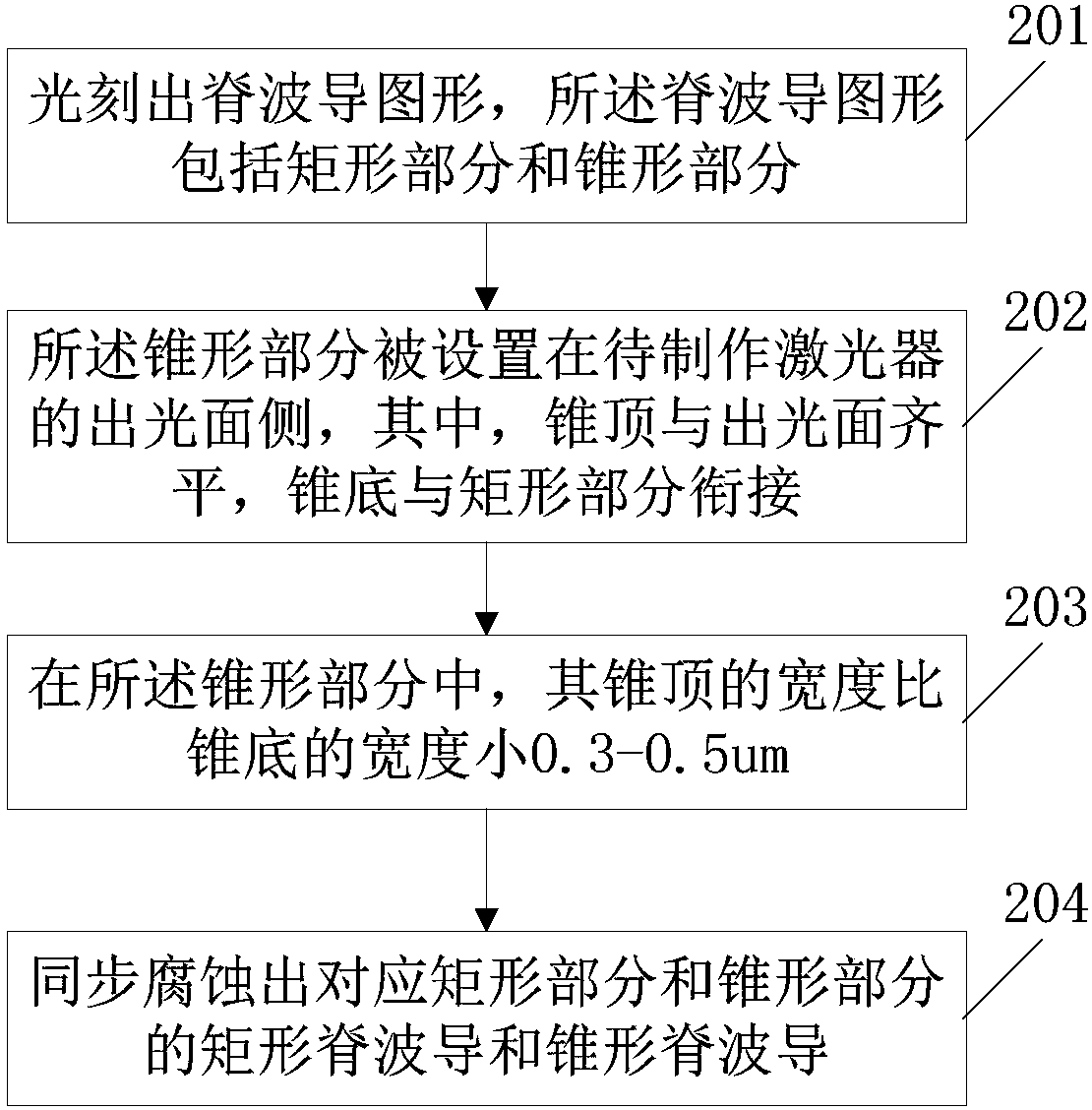
[0086] Embodiment 1 of the present invention provides a method for manufacturing a DFB laser. A buffer layer, a lower confinement layer, an active layer, an upper confinement layer, an etching stop layer, and a grating layer are fabricated on a substrate, and it is characterized in that, in the corrosion ridge waveguide, such as figure 2 As shown, the methods include:

[0087] In step 201, a ridge waveguide pattern is photoetched, and the ridge waveguide pattern includes a rectangular portion and a tapered portion.

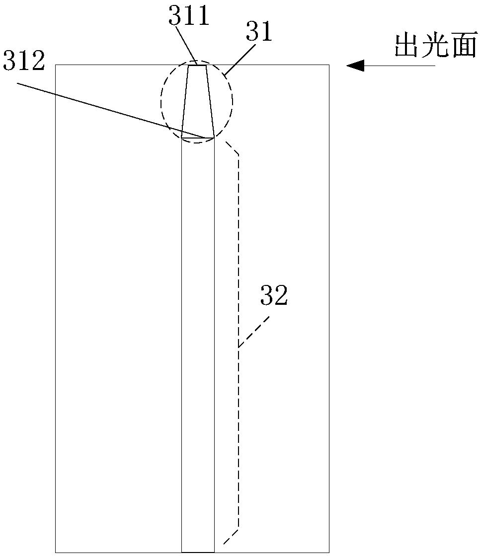
[0088] Such as image 3 As shown, a rectangular portion 32 and a tapered portion 31 in the ridge waveguide pattern are marked by a plan view and a dotted line frame.

[0089] In step 202, the tapered portion is arranged on the light-emitting surface side of the laser to be fabricated, wherein the cone top 311 is flush with the light-emitting surface, and the cone bottom 312 is connected to the rectangular portion.

[0090] In step 203, in the tapered part, the...

Embodiment 2

[0120] In the embodiment of the present invention, in addition to providing the DFB laser manufacturing method as described in Embodiment 1, a DFB laser structure completed by the manufacturing method described in Embodiment 1 is also provided, such as Figure 8 As shown, including substrate, buffer layer, lower confinement layer, active layer, upper confinement layer, etch stop layer and grating layer, specifically including:

[0121] An N-InP buffer layer 2 is grown on the InP substrate 1;

[0122] An N-InAlAs layer 3 and an InAlGaAs layer 4 with a graded Al composition are grown sequentially on the N-InP buffer layer 2;

[0123] growing a multi-quantum well active layer 5 on the graded layer;

[0124] On the multi-quantum well active layer 5, an InAlGaAs layer 6 and a P-InAlAs layer 7 with a graded Al composition are grown sequentially;

[0125] A P-InP space layer 8 and an etching stop layer 9 are sequentially grown on the P-InAlAs layer 7;

[0126] A ridge waveguide st...

Embodiment 3

[0130] In the embodiment of the present invention, in addition to providing the DFB laser manufacturing method as described in Embodiment 1, a DFB laser structure completed by the manufacturing method described in Embodiment 1 is also provided, such as Figure 7 As shown, the structure of each layer from bottom to top includes:

[0131] Substrate 1-0, which is an N-type InP layer;

[0132] a buffer layer 1-1, which is an N-type InP layer and formed on the substrate 1-0;

[0133] The first graded confinement layer 1-2, which is N-type InAl x Ga 1-x The As layer is formed on the buffer layer 1-1, x=0.5-0.1;

[0134] A first waveguide layer 1-3, which is an N-type InP layer and formed on the first graded confinement layer 1-2;

[0135] The second confinement layer 1-4, which is N-type InAl 0.5 Ga 0.5 An As layer is formed on the first waveguide layer 1-3;

[0136] The first quantum well barrier layer 1-5, which is non-doped Al 0.3 Ga 0.7 An InAs layer is formed on the se...


PUM

PropertyMeasurementUnit
Thicknessaaaaaaaaaa
Doping concentrationaaaaaaaaaa
Thicknessaaaaaaaaaa

Abstract

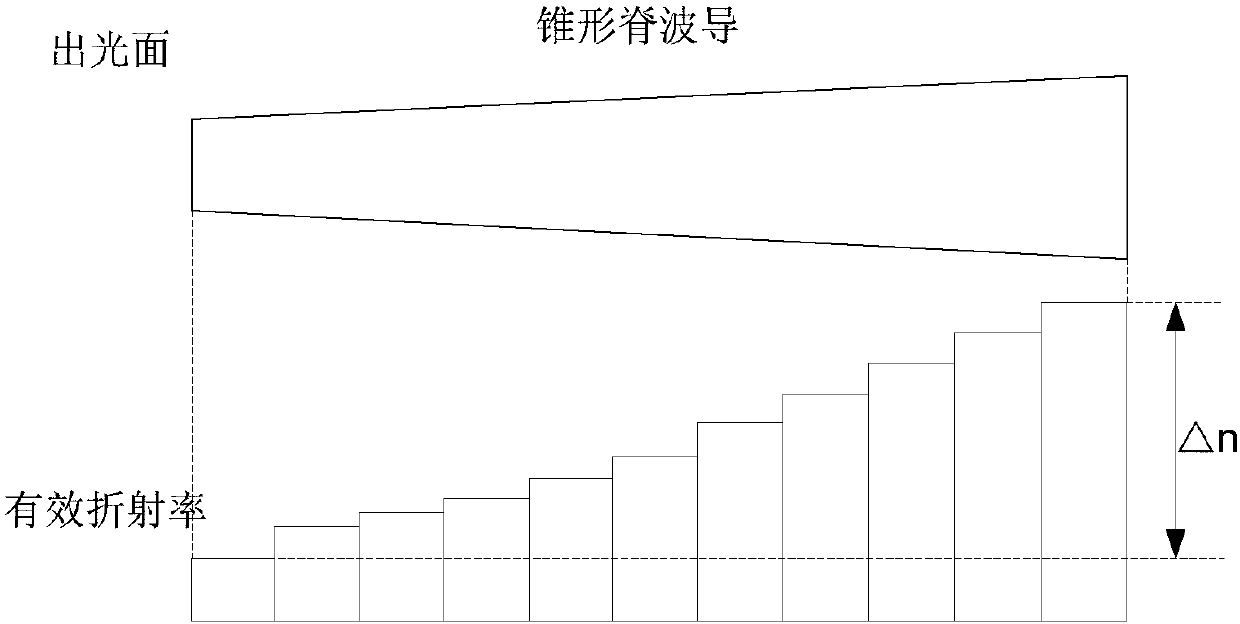
The invention relates to the technical field of lasers, and provides a DFB laser and a manufacturing method thereof. The manufacturing method comprises the steps of manufacturing a buffer layer, a lower limit layer, an active layer, an upper limiting layer, a corrosion stopping layer and a grating layer on a substrate, photoetching a ridge waveguide pattern including a rectangular part and a conical part when the ridge waveguide is etched, arranging the conical part on the light emitting surface side of the laser to be manufactured, wherein the conical top is flush with the light emitting surface, the conical bottom is connected with the rectangular part, and in the conical part, the width of the conical top is 0.3-0.5 micrometers smaller than the width of the conical bottom; synchronouslyetching the rectangular ridge waveguide and the conical ridge waveguide which correspond to the rectangular part and the conical part. The light with low wave length at the conical head is reflectedback to enter a cone bottom of a large light field limiting factor region, and the light with long wave length at the conical bottom is reflected back into the conical top of the small light field limiting factor region so as to be more easily emitted out. The conventional double-longitudinal mode is overcome, and the single-mode finished product rate of the laser can be effectively improved.

Description

【Technical field】 [0001] The invention relates to the technical field of lasers, in particular to a DFB laser and a manufacturing method thereof. 【Background technique】 [0002] Silicon-based semiconductors are the cornerstone of the modern microelectronics industry, but their development is nearing its limit. However, optoelectronic technology is in a stage of rapid development. The current semiconductor light-emitting devices are mostly made of compound materials, but they are not compatible with silicon microelectronics technology. Therefore, it is necessary to integrate optoelectronic technology and microelectronic technology to develop silicon-based optoelectronic science and technology. Significant. In recent years, the research on silicon-based optoelectronics has made remarkable and important breakthroughs at home and abroad, and all developed countries in the world have regarded silicon-based optoelectronics as their long-term development goals. With the increasin...

Claims


Application Information

Patent Timeline
IPC IPC(8): H01S5/12H01S5/343
CPCH01S5/12H01S5/343
Inventor 李亮刘应军刘巍王任凡
Owner WUHAN TELECOMM DEVICES
Learn More