Silicon wafer cleaning and texturing device

A silicon wafer cleaning and silicon wafer technology, which is applied in the directions of transportation and packaging, final product manufacturing, sustainable manufacturing/processing, etc., can solve the requirements that the temperature of the texturing solution cannot be guaranteed, watermarks are prone to appear, and the quality of silicon wafers is affected and other problems, to achieve the effect of convenient process adjustment, uniform heating temperature and guaranteed quality

Active Publication Date: 2018-04-27
LESHAN TOPRAYCELL
View PDF5 Cites 2 Cited by
  • Summary
  • Abstract
  • Description
  • Claims
  • Application Information

AI Technical Summary

Problems solved by technology

The existing texturing tanks are not stable enough to control the solution temperature, and cannot guarantee the solution temperature requirements for texturing
[0005] At the same time, in the prior art, although there is a device for continuous silicon wafer cleaning and texturing, during the process of transferring the silicon wafer from the cleaning solution to the texturing tank, the silicon wafer is prone to watermarks due to exposure to the air. As a result, the quality of silicon wafers is affected

Method used


Image

  • Silicon wafer cleaning and texturing device
  • Silicon wafer cleaning and texturing device
  • Silicon wafer cleaning and texturing device

Examples


Embodiment Construction

[0036] The present invention will be further described below in conjunction with the accompanying drawings and embodiments.

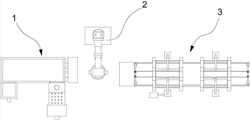
[0037] Such as Figure 1 to Figure 6 As shown, the silicon wafer cleaning and texturing device of the present invention includes a silicon wafer texturing tank 1, a silicon wafer transfer device 2 and a silicon wafer cleaning device 3; the silicon wafer transfer device 2 is arranged in the silicon wafer texturing tank 1 Between the silicon wafer cleaning device 3;

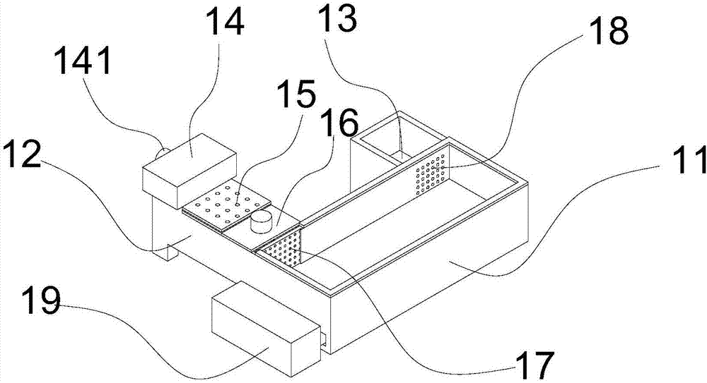
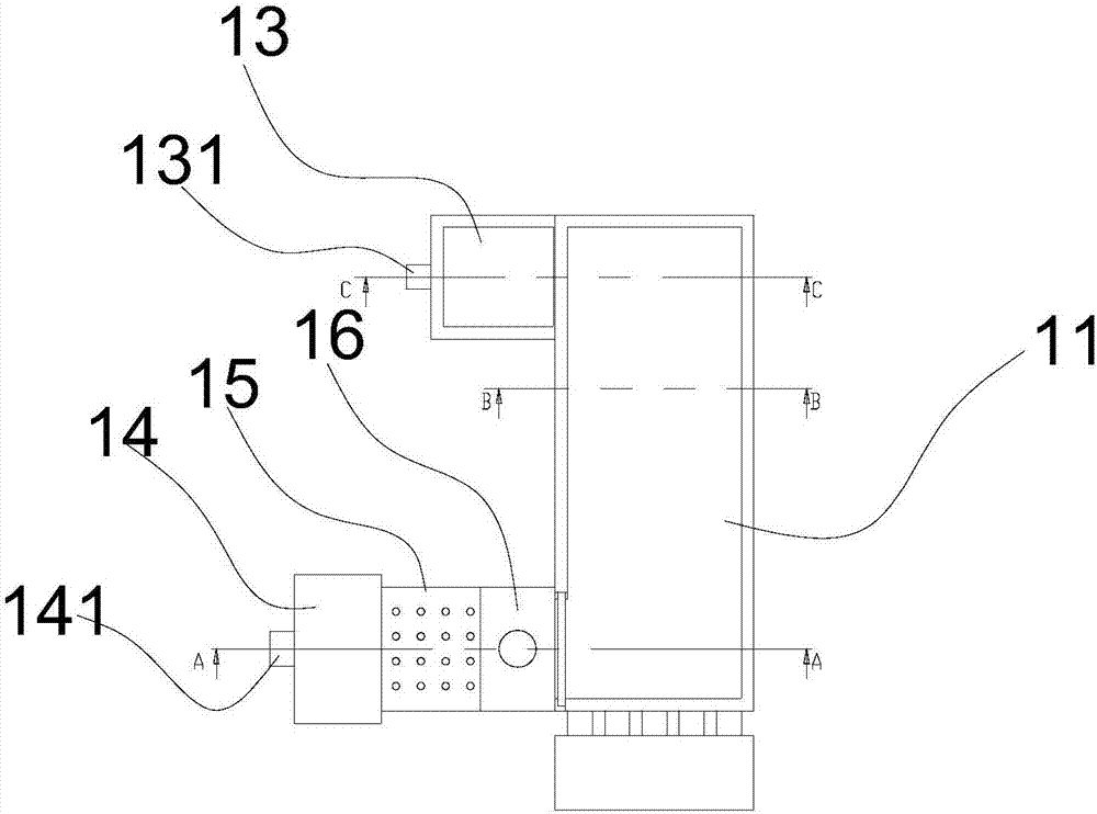
[0038] The silicon wafer texturing tank 1 includes a tank body 11 and a heating controller 19; one end of the tank body 11 is provided with a water inlet tank 12, and the other end is provided with a water outlet tank 13;

[0039] One end of the water inlet tank 12 is communicated with the tank body 11 through the first uniform flow plate 17, and the water inlet tank 14 communicated with the water inlet tank 12 is arranged above the other end; the water inlet tank 14 has a water inlet 141, ...


PUM


Abstract

The invention discloses a silicon wafer cleaning and texturing device, which can be convenient for texturing temperature control and ensure that a silicon wafer is always in a wet state when the silicon wafer undergoes the silicon wafer cleaning and texturing processes. The silicon wafer cleaning and texturing device comprises a silicon wafer texturing trough, a silicon wafer transfer device and asilicon wafer cleaning device, wherein the silicon wafer transfer device is arranged between the silicon wafer texturing trough and the silicon wafer cleaning device. By adopting the silicon wafer cleaning and texturing device, the texturing temperature control precision is high, the chemical reaction in the entire process tank is stable and controllable, effective control of the reaction speed and volatilization amount of a solution can be realized, and the adjustment of the process is facilitated; and the silicon wafer is sprayed during the transfer process so as to ensure that the siliconwafer always maintains a wet state during operation, thereby effectively avoiding the occurrence of ''edge scratched wafer'', and improving product quality.

Description

technical field [0001] The invention relates to silicon chip texturing, in particular to a silicon chip cleaning and texturing device. Background technique [0002] It is well known that silicon wafers need to be cleaned after a series of processing procedures. The purpose of cleaning is to eliminate all kinds of pollutants adsorbed on the surface of silicon wafers, and to make a suede structure that can reduce the reflection of sunlight on the surface. The degree of cleanliness directly affects the yield and reliability of cells. Texturing is the first process for manufacturing crystalline silicon cells, also known as "surface texturing". The effective textured structure makes the incident light reflect and refract multiple times on the surface of the silicon wafer, which increases the light absorption, reduces the reflectivity, and helps to improve the performance of the battery. [0003] Considering the important role of the texturing process section on the entire produ...

Claims


Application Information

Patent Timeline
Patent Type & Authority Applications(China)
IPC IPC(8): H01L21/67H01L21/677H01L31/0236H01L31/18C30B29/06C30B33/10
CPCC30B29/06C30B33/10H01L21/67086H01L21/67109H01L21/67703H01L31/02366H01L31/1804Y02P70/50
Inventor 陈五奎刘强徐文州
Owner LESHAN TOPRAYCELL
Why Eureka
Try Eureka