led package structure
A technology of LED packaging and packaging structure, which is applied in the direction of semiconductor devices, electrical components, circuits, etc., and can solve the problems of reducing the light extraction efficiency of packaging, the aging of packaging glue, and the reduction of light intensity, etc.
- Summary
- Abstract
- Description
- Claims
- Application Information
AI Technical Summary
Problems solved by technology
Method used
Image
Examples
Embodiment 1
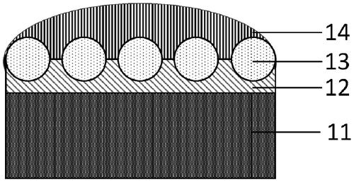
[0036] See figure 1 , figure 1 A schematic diagram of the LED package structure provided for an embodiment of the present invention, including:
[0037] LED base plate 11;
[0038] The first silica gel layer 12 is arranged on the LED bottom plate 11;
[0039] The lens area 13 is arranged on the first silica gel layer 12;
[0040] The second silica gel layer 14 is disposed on the first silica gel layer 12 and the lens area 13 .
[0041] Specifically, the silica gel refractive index of the first silica gel layer 12 is smaller than that of the second silica gel layer 14 , and the silica gel refractive index of the lens region 13 is greater than the silica gel refractive index of the first silica gel layer 12 and the second silica gel layer 14 .
[0042] Specifically, the LED bottom plate 11 includes a heat dissipation substrate and LED chips disposed on the heat dissipation substrate.
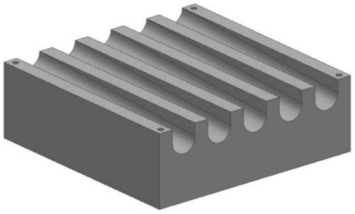
[0043] Further, see figure 2 , figure 2 It is a schematic diagram of an LED package h...
Embodiment 2
[0055] Please refer to Figure 4 , Figure 4 The flow chart of the LED packaging method provided by another embodiment of the present invention, this embodiment is based on the above-mentioned embodiments, and the packaging method of the LED packaging structure of the present invention is described in detail as follows. Specifically, include the following steps:
[0056] S21, selecting LED chips;
[0057] S22, selecting a bracket and a heat dissipation substrate;
[0058] S23. Welding the LED chip to the heat dissipation substrate;
[0059] S24. Coating a first silica gel layer on the LED chip;
[0060] S25, configuring fluorescent powder glue;
[0061] S26, preparing the lens area;
[0062] S27. Coating an outer phosphor glue on the lens area; and forming a second silica gel layer on the outer phosphor glue by using a hemispherical mold; to complete the LED package.
[0063] Preferably, the LED chip is an ultraviolet LED chip.
[0064] Specifically, step S22 may inclu...
Embodiment 3
[0096] Further, please refer to Figure 6 , Figure 6 It is a schematic diagram of a high-transmittance LED package structure provided in another embodiment of the present invention. The LED package structure provided in this embodiment is prepared by the method provided in the above-mentioned embodiments. Specifically, the LED packaging structure includes: a heat dissipation substrate 31 , an LED chip 32 , a first silica gel layer 33 , a lens area 34 and a second silica gel layer 35 from bottom to top.
[0097] Specifically, the first silica gel layer 33 is silica gel without phosphor; wherein, the first silica gel layer 33 does not contain phosphor, which separates the phosphor from the LED chip, and solves the problem of reduced quantum efficiency of the phosphor caused by high temperature.
[0098] Specifically, the refractive index of the first silica gel layer 33 , the second silica gel layer 35 and the silica gel in the lens area 34 increases sequentially.
[0099] Wh...
PUM
| Property | Measurement | Unit |
|---|---|---|
| diameter | aaaaa | aaaaa |
| thickness | aaaaa | aaaaa |
| thickness | aaaaa | aaaaa |
Abstract
Description
Claims
Application Information


