A kind of led packaging structure
A technology of LED encapsulation and silica gel layer, which is applied in the direction of semiconductor devices, electrical components, circuits, etc., can solve the problems of insufficient concentration of light source illumination, influence of light transmission efficiency, and reduction of light intensity, so as to suppress total reflection effect, reduce cost, The effect of increasing the cooling effect
- Summary
- Abstract
- Description
- Claims
- Application Information
AI Technical Summary
Problems solved by technology
Method used
Image
Examples
Embodiment 1
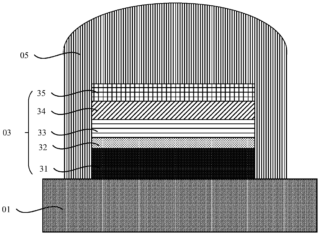
[0043] See figure 1 , figure 1 It is a schematic diagram of an LED package structure provided by an embodiment of the present invention. The structure includes:
[0044] Heat dissipation substrate 01;
[0045] The ultraviolet wick 03 is arranged on the upper surface of the heat dissipation substrate;
[0046] The silica gel layer 05 is disposed on the heat dissipation substrate and the upper surface of the ultraviolet wick.
[0047] Wherein, the heat dissipation substrate 01 is made of copper.
[0048] Further, circular grooves along the width direction and parallel to the plane of the heat dissipation substrate are provided on the outer side of the heat dissipation substrate 01; wherein, the diameter of the circular grooves is 0.3-2 mm, and the distance between the circular grooves is 0.5-10 mm.
[0049] Wherein, the ultraviolet wick 03 includes an n-AlGaN layer 32, an MQW layer 33, a p-AlGaN layer 34, and a p-GaN layer 35 arranged on the surface of the sapphire substrat...
Embodiment 2
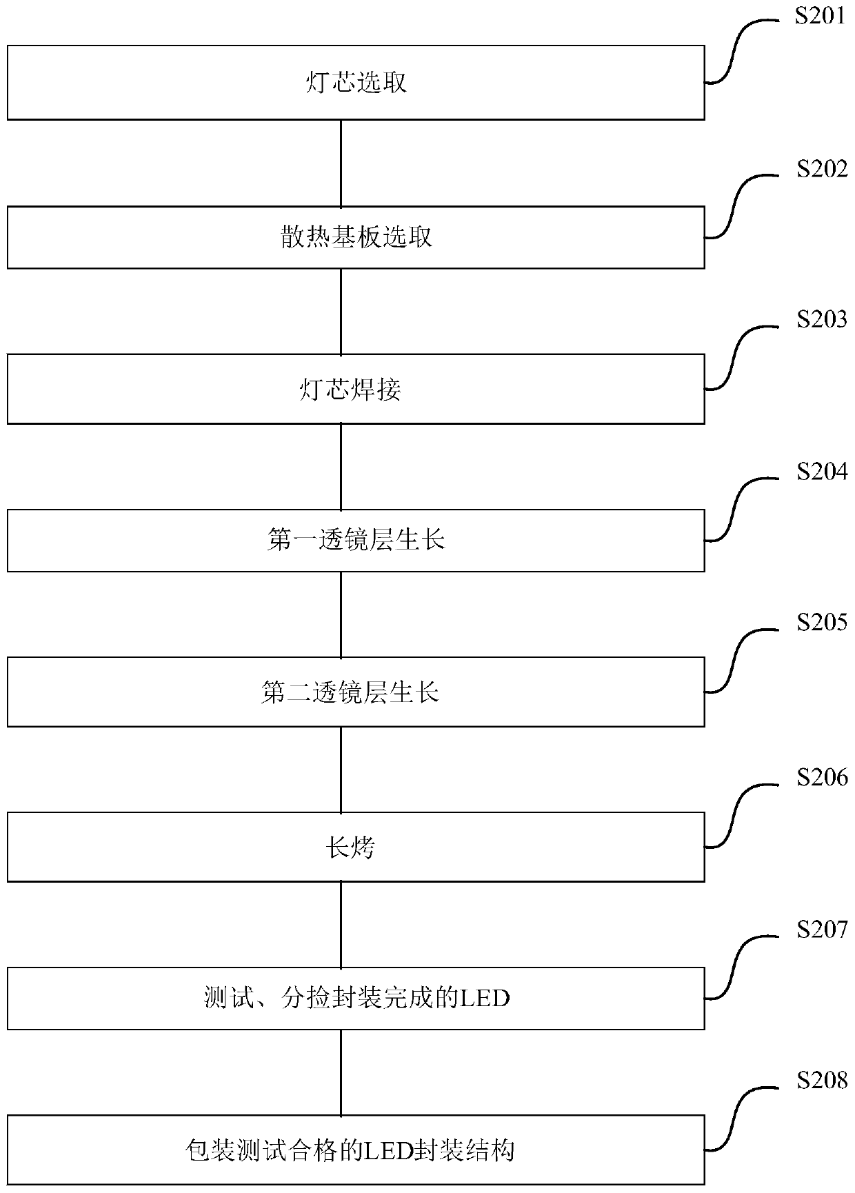
[0066] See figure 2 , figure 2 It is a flowchart of a double-layer lens layer LED packaging method provided by an embodiment of the present invention. On the basis of the above embodiments, this embodiment will introduce in detail the process flow of the double-layer lens layer LED package proposed by the present invention. The method includes:
[0067] S201. Wick selection
[0068] Select the ultraviolet wick as the wick of the LED.
[0069] S202. Selection of heat dissipation substrate
[0070] Only a part of the energy in the LED input power is converted into light energy, and the rest is converted into heat energy. Therefore, for LED chips, especially LED chips with high power density, how to control their thermal energy is an important issue that LED manufacturing and lamps should focus on solving. The heat of high-power diodes, high-power triodes, IGBTs, and MOSFETs can be dissipated through an external radiator with almost unlimited size installed on the instrum...
Embodiment 3
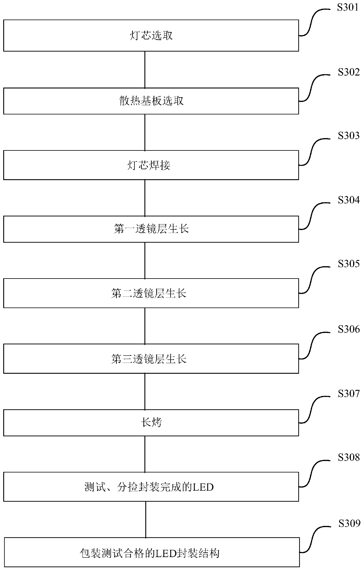
[0115] See image 3 , image 3 It is a flow chart of a three-layer lens layer LED packaging method provided by an embodiment of the present invention. On the basis of the above embodiments, this embodiment will introduce in detail the process flow of the three-layer lens layer LED package proposed by the present invention. include:
[0116] S301. Wick selection
[0117] Select the ultraviolet wick as the wick of the LED.
[0118] S302. Selection of heat dissipation substrate
[0119] S3021, bracket / radiation substrate preparation
[0120] Metal copper is selected as the material of the heat dissipation substrate, and the thickness of the heat dissipation substrate is 0.5-10mm. The outer side of the heat dissipation substrate has circular grooves along the width direction and parallel to the plane of the heat dissipation substrate; wherein, the diameter of the circular grooves is 0.3-2mm, and the distance between the circular grooves is 0.5-10mm. The circular groove can ...
PUM
 Abstract
Description
Claims
Application Information


