Capacitive coupling of integrated circuit die components
An integrated circuit and capacitive technology, applied in the direction of circuits, electrical components, electric solid devices, etc., to achieve low voltage requirements, material saving, and low operating voltage
- Summary
- Abstract
- Description
- Claims
- Application Information
AI Technical Summary
Problems solved by technology
Method used
Image

Examples
Embodiment Construction
[0015] exemplary system
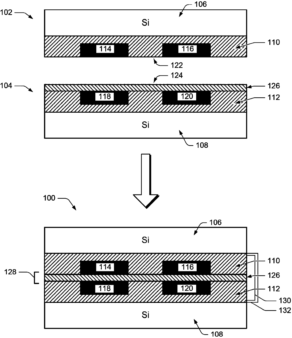
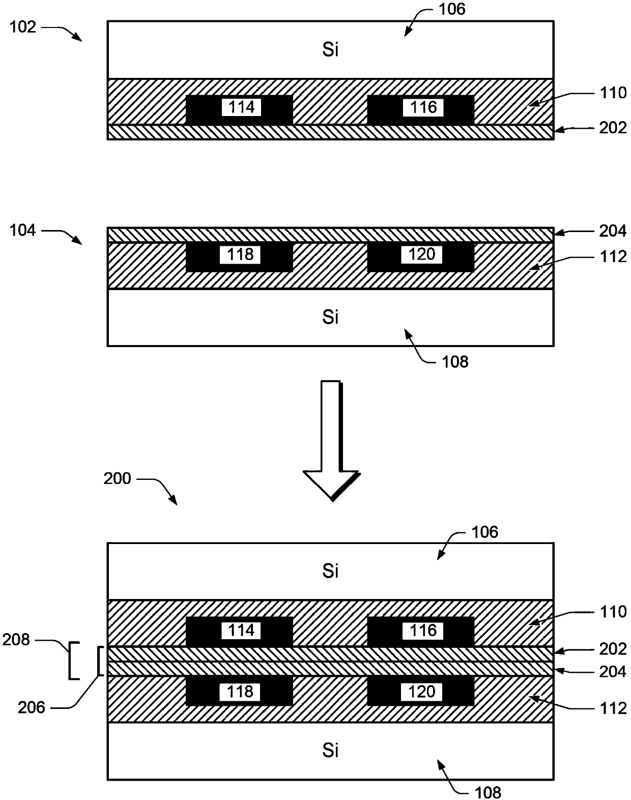
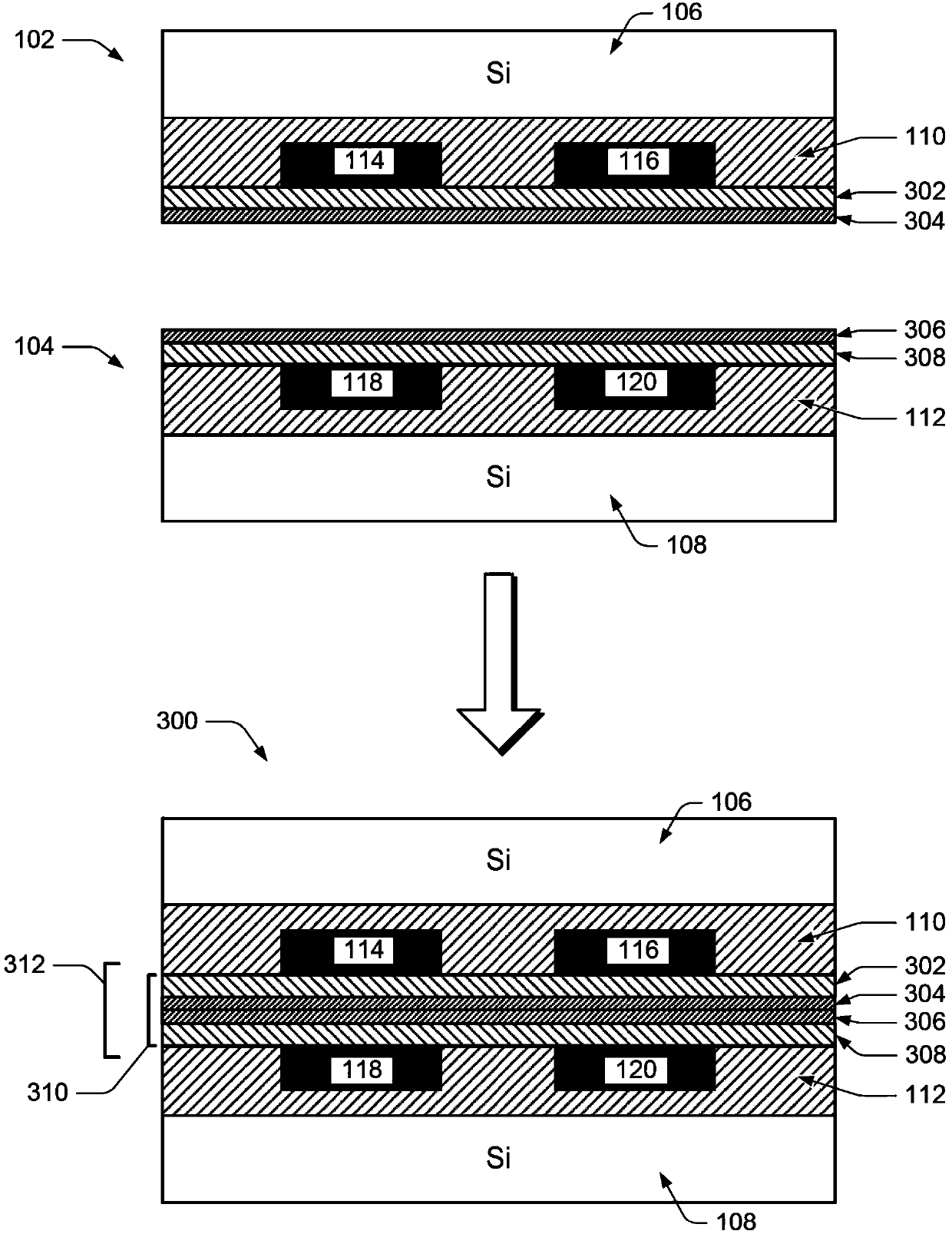
[0016] figure 1 An exemplary wafer level packaging structure 100 including a first integrated circuit die 102 and a second integrated circuit die 104 is shown. Each integrated circuit die 102, 104 has a semiconductor 106, 108 (eg, silicon) and an underfill layer 110, 112 made of an insulator or dielectric (eg, silicon dioxide) to secure conductive regions 114, 116 and 118, 120. Each integrated circuit die 102 , 104 has a respective surface 122 , 124 that includes at least one of the conductive regions 114 , 116 or 118 , 120 .
[0017] The ultra-thin dielectric layer 126 has a thickness less than or equal to about 50 nanometers, and the ultra-thin dielectric layer 126 is formed on at least one of the surfaces 122 or 124 of at least one of the integrated circuit dies 102, 104 . The ultra-thin dielectric layer can be a coating, film, residue, film, deposit...etc. The coupled stack 100 forms a capacitive interface 128 comprising the ultra-thin dielec...
PUM
 Abstract
Description
Claims
Application Information
 - R&D
- Intellectual Property
- Life Sciences
- Materials
- Tech Scout
- Unparalleled Data Quality
- Higher Quality Content
- 60% Fewer Hallucinations
Browse by: Latest US Patents, China's latest patents, Technical Efficacy Thesaurus, Application Domain, Technology Topic, Popular Technical Reports.
© 2025 PatSnap. All rights reserved.Legal|Privacy policy|Modern Slavery Act Transparency Statement|Sitemap|About US| Contact US: help@patsnap.com