Bilayer glue stripping process applying flood exposure through acoustic surface wave filter

A technology of surface acoustic wave and peeling process, which is applied in the photoengraving process of pattern surface, photosensitive material processing, microlithography exposure equipment, etc. For independence, complexity of process details, etc.

Inactive Publication Date: 2018-05-15
ZHEJIANG HUAYUAN MICRO ELECTRONICS TECH CO LTD
View PDF4 Cites 5 Cited by
  • Summary
  • Abstract
  • Description
  • Claims
  • Application Information

AI Technical Summary

Problems solved by technology

However, the general use of double-layer glue stripping process has strict requirements on photoresist sensitivity, independence of

Method used


Image

  • Bilayer glue stripping process applying flood exposure through acoustic surface wave filter
  • Bilayer glue stripping process applying flood exposure through acoustic surface wave filter

Examples


Embodiment 1

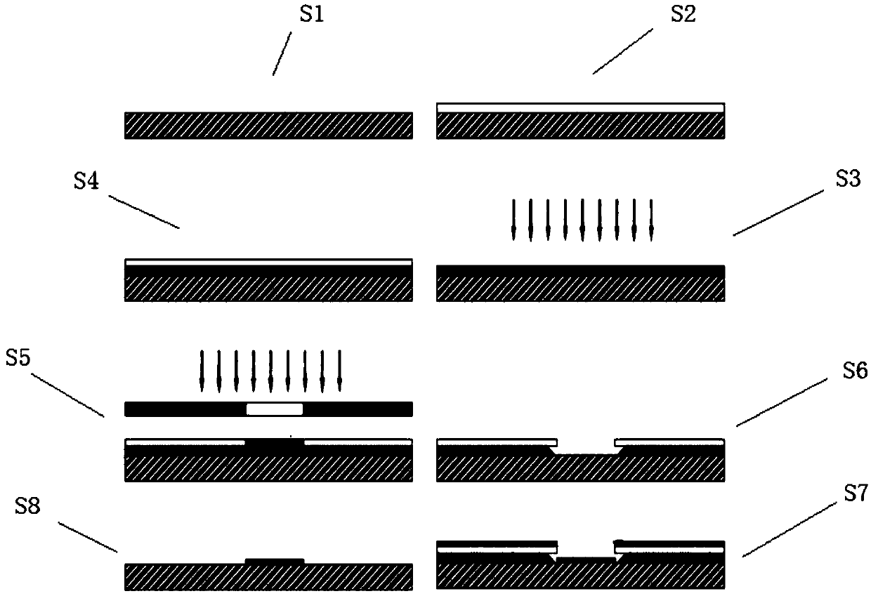
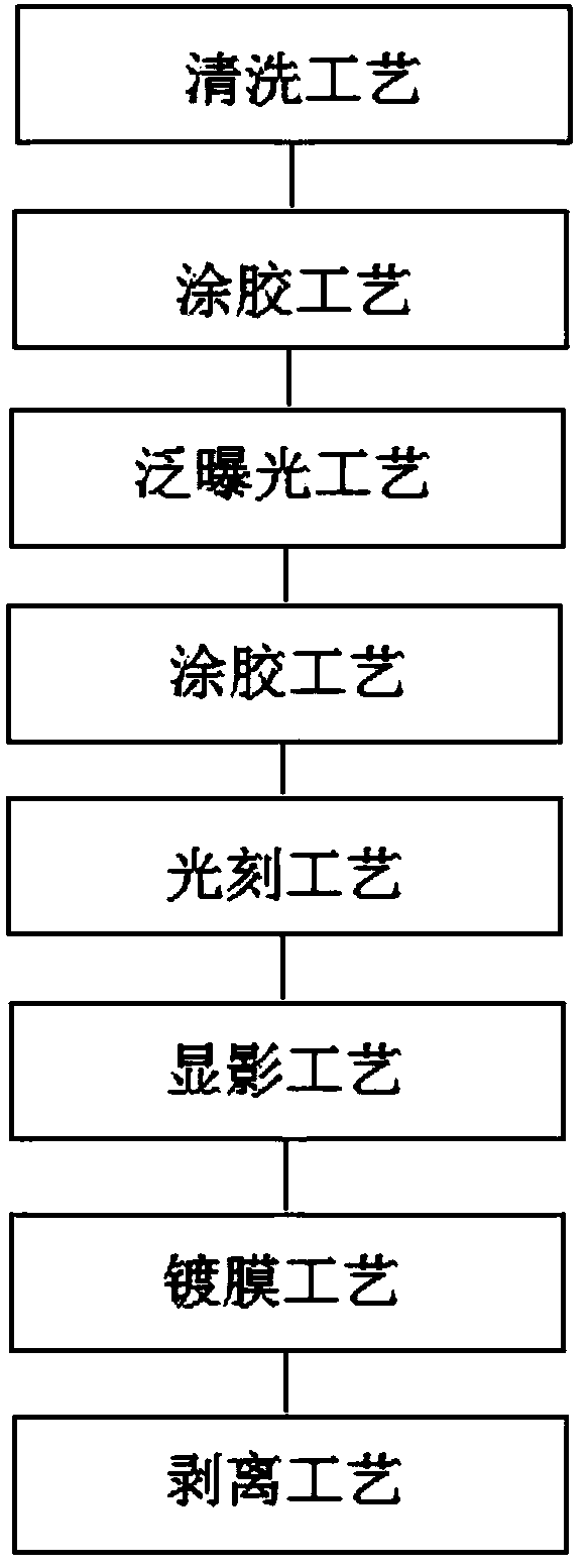
[0026] combine figure 1 , figure 2 As shown, the specific steps of the double-layer adhesive peeling process of applying flood exposure to the surface acoustic wave filter are described in detail as follows.

[0027] Step 1. Cleaning process: cleaning of piezoelectric materials.

[0028] Step 2. Coating process: Spin-coat an ordinary positive photoresist with a viscosity of 49 CPS at a rotational speed of 5000 rpm, and a thickness of about 22000 angstroms.

[0029] Step 3. Pan-exposure treatment: UV flood exposure (full exposure of all non-mask plates without difference on the entire wafer) irradiates the wafer coated with positive photoresist, the photoresist is completely exposed, and the photoresist reacts.

[0030] Step 4. Secondary coating process: In order to prevent the first layer of photoresist from collapsing, spin-coat a positive photoresist with a viscosity of 14CPS at a speed of 3000 rpm (need to be the same as the photoresist with a viscosity of 49CPS used in ...

Embodiment 2

[0039] Step 1. Cleaning process: cleaning of piezoelectric materials.

[0040] Step 2. Coating process: Spin-coat ordinary positive photoresist with a viscosity of 45CPS at a rotational speed of 5500 rpm, and a thickness of about 20000 angstroms.

[0041] Step 3. Pan-exposure treatment: UV flood exposure (full exposure of all non-mask plates without difference on the entire wafer) irradiates the wafer coated with positive photoresist, the photoresist is completely exposed, and the photoresist reacts.

[0042] Step 4. Second coating process: In order to prevent the first layer of photoresist from collapsing, spin-coat a positive photoresist with a viscosity of 13CPS at a speed of 3000 rpm (need to be the same as the photoresist with a viscosity of 45CPS used in the second step) The model is the same as the name of the product, so the same developer can be used), and the thickness of the glue is about 14000 angstroms.

[0043] Step 5. Photolithography process: Ultraviolet rays ...

Embodiment 3

[0048] 1. Cleaning process: Soak in concentrated sulfuric acid + hydrogen peroxide for 4 hours to remove organic matter and metal impurities in the piezoelectric material, and remove tiny particles by rinsing and megasonic cleaning to complete the cleaning of the piezoelectric material wafer.

[0049] 2. Glue coating process: Spin-coat ordinary positive photoresist with a viscosity of 49CPS at a speed of 5000 rpm, heat on a hot plate at 90°C for 90 seconds, and the thickness of the glue is about 22000 angstroms.

[0050] 3. Pan-exposure treatment: Use URE-2000 / 35 deep ultraviolet lithography machine to perform pan-exposure on the piezoelectric material (full exposure of the entire wafer with no mask and no difference), the time is 5 minutes, and the photoresist The exposure is complete and the photoresist reacts.

[0051] 4. Second coating process: In order to prevent the first layer of photoresist from collapsing, spin-coat positive photoresist with a viscosity of 14CPS at a ...


PUM

PropertyMeasurementUnit
Viscosityaaaaaaaaaa

Abstract

The invention relates to the technical field of electricity and nano processing, in particular to a bilayer glue stripping process applying flood exposure through an acoustic surface wave filter. Theprocess includes following steps: step 1, cleaning: cleaning the surface of a piezoelectric material; step 2, gluing: smearing a first layer of positive photoresist of 49CPS in viscosity on the surface of the piezoelectric material; step 3, performing flood exposure: using ultraviolet to perform whole mask-free undifferentiated sufficient exposure on a whole wafer, and irradiating the piezoelectric material coated with the positive photoresist, wherein the photoresist reacts after exposure of the photoresist is completed; step 4, gluing for the second time: smearing a second layer of positivephotoresist of 14CPS in viscosity on the surface of the positive photoresist; step 5, photoetching: allowing ultraviolet to penetrate a photolithography photic zone to irradiate the piezoelectric material, wherein an area of the second layer of the positive photoresist contacting with the ultraviolet reacts; step 6, developing; step 7, coating: selecting proper coating equipment to perform evaporation coating; step 8, stripping.

Description

technical field [0001] The invention relates to the technical fields of electricity and nano-processing, in particular to a double-layer glue stripping process using pan-exposure for a surface acoustic wave filter. Background technique [0002] With the advent of the new generation of mobile communications, surface acoustic wave filters (SAWF) are widely used in radio frequency mobile communications. The technology of surface acoustic wave chips is developing rapidly, and new research and new discoveries of technology have become an important focus. [0003] The traditional double-layer adhesive stripping process uses an "inverted trapezoidal" structure with a narrow top and a wide bottom (such as figure 1 shown), which reduces the difficulty of metal stripping and improves the efficiency of stripping. However, the general use of double-layer glue stripping process has strict requirements on photoresist sensitivity, independence of developer, and complexity of process detai...

Claims


Application Information

Patent Timeline
IPC IPC(8): G03F7/20G03F7/42
CPCG03F7/2022G03F7/422
Inventor 刘绍侃张少华李善斌蒋燕港
Owner ZHEJIANG HUAYUAN MICRO ELECTRONICS TECH CO LTD
Why Eureka
Try Eureka