Shield gate trench MOSFET and manufacturing method thereof

A manufacturing method and technology for shielding gates, which are applied in semiconductor/solid-state device manufacturing, electrical components, circuits, etc., can solve the problems of increasing leakage between gate and source, leakage, and gate-source leakage, and achieve the effect of reducing leakage and eliminating leakage.

Inactive Publication Date: 2018-05-15
SHANGHAI HUAHONG GRACE SEMICON MFG CORP
View PDF5 Cites 18 Cited by
  • Summary
  • Abstract
  • Description
  • Claims
  • Application Information

AI Technical Summary

Problems solved by technology

It can be seen that, in order to obtain a low threshold voltage device, it is necessary to use a thinner gate oxide layer 104, and a thinner gate oxide layer 104 will simultaneously reduce the thickness of the isolation oxide layer 104a between polysilicon, thereby increasing the leakage between the gate and source. , so the existing method cannot solve the contradiction between lowering the threshold voltage and reducing the gate-source leakage
[0021] In addition, the device formed by the existing method also has the above-mentioned thickness of the isolation oxide layer 104a between polysilicon at the corner shown by the dotted circle 205 is thinner than that of other regions, which makes it easy to generate a gate-source gap at the dotted circle 205. Leakage between
And the sharp corner defects in the area shown by the dotted circle 204 are also easy to generate leakage between the gate and source

Method used


Image

  • Shield gate trench MOSFET and manufacturing method thereof
  • Shield gate trench MOSFET and manufacturing method thereof
  • Shield gate trench MOSFET and manufacturing method thereof

Examples


Embodiment Construction

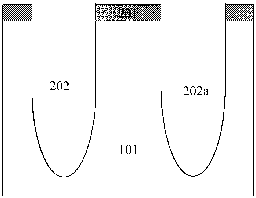
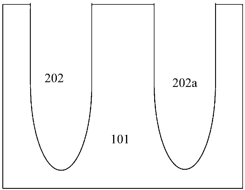
[0077] like figure 2 As shown, it is a schematic structural diagram of the shielded gate trench MOSFET of the embodiment of the present invention; the conduction region of the shielded gate trench MOSFET of the embodiment of the present invention is composed of a plurality of primitive cells arranged periodically, and each primitive cell of the conduction region is Including a gate structure, the gate structure of the shielded gate trench MOSFET in the embodiment of the present invention is a top and bottom structure, and a gate lead-out area is also provided outside the conduction area. figure 2 The gate lead-out area is also shown in . The gate structure includes:

[0078] In the trench formed in the semiconductor substrate 1 , a bottom oxide layer 2 is formed on the side and bottom surface of the trench, and the shielding polysilicon 3 completely fills the trench formed with the bottom oxide layer 2 .

[0079] Preferably, the semiconductor substrate 1 is a silicon subst...


PUM


Abstract

The invention discloses a shield gate trench MOSFET. A bottom oxide layer is formed on the side surface and the bottom surface of the trench of a gate structure, and shield polysilicon totally fills the trench; under self-alignment definition of the bottom oxide layer, the shield polysilicon is etched back to the bottom part of the trench in a self-alignment mode; the surface of the shield polysilicon after self-alignment etching back is oxidized to form an inter-polysilicon isolated oxide layer; after the inter-polysilicon isolated oxide layer is formed, the bottom oxide layer is etched backto the bottom part of the trench, the bottom oxide layer after etching back and the inter-polysilicon isolated oxide layer surround the shield polysilicon, and a top trench is formed at the top part of the trench; and the side surface of the top trench is provided with a gate oxide layer and is filled with polysilicon gate. The invention also discloses a manufacturing method for the shield gate trench MOSFET. Gate source electric leakage of the device can be reduced while the threshold voltage of the device is reduced, the thickness consistency of the inter-polysilicon isolated oxide layer canbe improved, and the capacitor corresponding to the inter-polysilicon isolated oxide layer is stable and controllable.

Description

technical field [0001] The invention relates to the field of manufacturing semiconductor integrated circuits, in particular to a shield gate (Shield Gate Trench, SGT) trench MOSFET; the invention also relates to a manufacturing method of the shield gate trench MOSFET. Background technique [0002] like Figure 1A to Figure 1P As shown, it is a schematic diagram of the device structure in each step of the manufacturing method of the existing shielded gate trench MOSFET; this method forms a shielded gate trench gate structure with an upper and lower structure. Usually, the conduction region of the shielded gate trench MOSFET is composed of multiple Each primitive cell in the conduction region includes a gate structure. In the shielded gate trench gate structure with an up-and-down structure, a gate lead-out area, including a gate lead-out area, needs to be set. The formation steps are as follows: [0003] Step 1, such as Figure 1A As shown, a semiconductor substrate such as...

Claims


Application Information

Patent Timeline
Patent Type & Authority Applications(China)
IPC IPC(8): H01L29/78H01L29/423H01L29/06H01L21/336
CPCH01L29/0653H01L29/4236H01L29/66553H01L29/66666H01L29/7827H01L29/7813H01L29/407H01L29/41766H01L29/66734
Inventor 范让萱
Owner SHANGHAI HUAHONG GRACE SEMICON MFG CORP
Why Eureka
Try Eureka