A wafer bonding method based on pre-trimming process

A wafer bonding and wafer technology, applied in the direction of semiconductor devices, electrical components, circuits, etc., can solve problems affecting the bonding process, etc., to improve product performance, reduce defect rate, and increase product yield.

Active Publication Date: 2019-07-02
WUHAN XINXIN SEMICON MFG CO LTD
View PDF4 Cites 0 Cited by
  • Summary
  • Abstract
  • Description
  • Claims
  • Application Information

AI Technical Summary

Problems solved by technology

[0007] How to avoid the residue generated in the previous process from affecting the subsequent bonding process has become an urgent technical problem to be solved

Method used


Image

  • A wafer bonding method based on pre-trimming process
  • A wafer bonding method based on pre-trimming process
  • A wafer bonding method based on pre-trimming process

Examples


Embodiment Construction

[0038] It should be noted that, in the case of no conflict, the following technical solutions and technical features can be combined with each other.

[0039] The specific embodiment of the present invention will be further described below in conjunction with accompanying drawing:

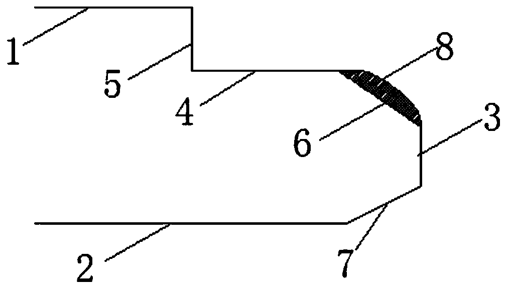
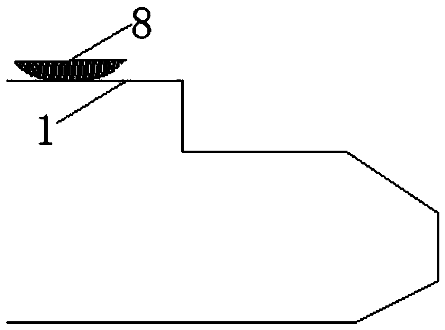
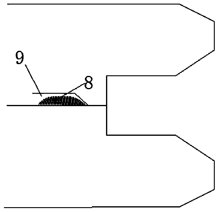
[0040] Such as Figure 4 , 6 As shown in -8, a wafer bonding method based on a pre-trimming process, the above-mentioned wafer bonding method is applicable to two wafers processed by the previous process technology respectively, and the edges of one or two of the above-mentioned wafers have respectively A chamfer, the above-mentioned chamfer has a residue 8' produced after the above-mentioned pre-production process; it is characterized in that the above-mentioned wafer bonding method includes:

[0041] Step S1, performing a pre-trimming process on one or two wafers having the above-mentioned chamfers through a pre-trimming process to remove the above-mentioned residue 8' on the above-mentioned wa...


PUM


Abstract

The invention provides a wafer bonding method based on a pre-trimming process, which belongs to the technical field of semiconductor manufacturing, and includes: step S1, performing pre-trimming treatment on one or two wafers through a pre-trimming process to remove residues on the wafers ; Step S2, through the bonding process, two wafers are bonded so that the two wafers are bonded; in step S1, the specific steps of pre-trimming processing through the pre-trimming process include: Step S11, through a trimming The grinding head of the equipment grinds the residue on the chamfer to remove the residue; step S12 , cleaning the wafer at least once with an acid solution. The beneficial effect of the present invention: it can remove the residues generated in the previous manufacturing process, avoid the residues from peeling off to the surface of the wafer during the bonding process, and form bonding defects after the wafers are bonded, thereby reducing the wafer bonding void defect rate and improving Product yield, improve product performance.

Description

technical field [0001] The invention relates to the technical field of semiconductor manufacturing, in particular to a wafer bonding method based on a pre-trimming process. Background technique [0002] In integrated circuit processing, 3D integration is a solution to improve chip performance while maintaining existing technology nodes. The performance of the chip can be improved by three-dimensional integration of two or more chips with the same or different functions. At the same time, the metal interconnection between functional chips can be greatly shortened, and heat generation, power consumption and delay can be reduced. [0003] In the three-dimensional integration process, the wafer-to-wafer bonding process is the core focus, and the wafer bonding void defect rate is the core parameter to measure the wafer bonding process. [0004] The wafer bonding void defect rate in the three-dimensional integration process is an important factor affecting the overall defect rate...

Claims


Application Information

Patent Timeline
Patent Type & Authority Patents(China)
IPC IPC(8): H01L21/60
CPCH01L24/01
Inventor 邹文
Owner WUHAN XINXIN SEMICON MFG CO LTD
Why Eureka
Try Eureka