OLED unit and manufacturing method thereof, display panel and display device

A technology for display panels and substrate substrates, which is applied to electrical components, semiconductor devices, circuits, etc., can solve the problems of complex manufacturing processes of display panels, and achieve the effect of simplifying manufacturing processes and reducing manufacturing costs.

Pending Publication Date: 2018-05-18
BOE TECH GRP CO LTD +1
View PDF0 Cites 18 Cited by
  • Summary
  • Abstract
  • Description
  • Claims
  • Application Information

AI Technical Summary

Problems solved by technology

[0005] The invention provides an OLED unit, a manufacturing method thereof, a display panel, and a display device, which can solve the problem that additional The manuf...

Method used


Image

  • OLED unit and manufacturing method thereof, display panel and display device
  • OLED unit and manufacturing method thereof, display panel and display device
  • OLED unit and manufacturing method thereof, display panel and display device

Examples


Embodiment Construction

[0036] In order to make the object, technical solution and advantages of the present invention clearer, the implementation manner of the present invention will be further described in detail below in conjunction with the accompanying drawings.

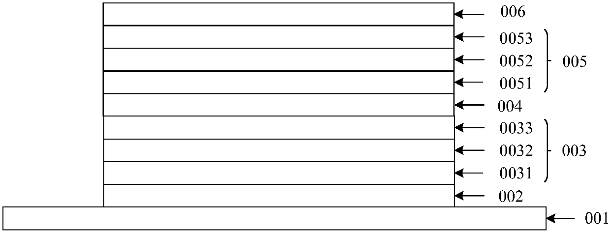
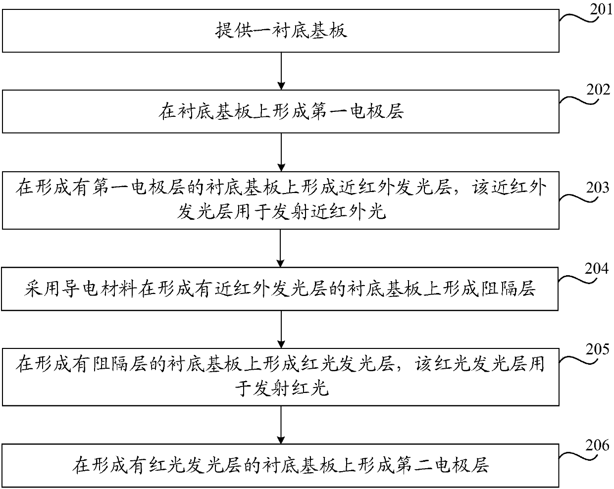
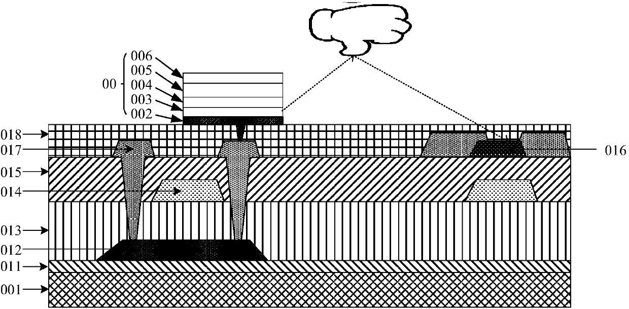
[0037] figure 1 It is a schematic structural diagram of an OLED unit provided by an embodiment of the present invention, such as figure 1 As shown, the OLED unit may include:

[0038] The first electrode layer 002 is disposed on the base substrate 001.

[0039] The near-infrared light-emitting layer 003 disposed on the side of the first electrode layer 002 away from the base substrate 001, the near-infrared light-emitting layer 003 is used to emit near-infrared light, and the near-infrared light can be emitted to the surface of the finger pressed on the surface of the display panel , and reflected by the finger into the photoelectric conversion component, the photoelectric conversion component can convert the received near-infrared l...


PUM


Abstract

The invention discloses an OLED unit and a manufacturing method thereof, a display panel and a display device, and belongs to the technical field of display. The OLED unit includes a first electrode layer disposed on a substrate base plate, a near-infrared emitting layer, a barrier layer, a red light emitting layer and a second electrode layer. The near-infrared emitting layer is disposed on the side, away from substrate base plate, of the first electrode layer and used for emitting near-infrared light; the barrier layer is disposed on the side, away from the substrate base plate, of the near-infrared emitting layer and made of a conductive material; the red light emitting layer is disposed on the side, away from the substrate base plate, of the barrier layer and used for emitting red light; the second electrode layer is disposed on the side, away from the substrate base plate, of the red light emitting layer, and the polarity of the second electrode layer is opposite to that of the first electrode layer. The manufacturing process of the display panel is simplified, and the manufacturing cost is reduced.

Description

technical field [0001] The invention relates to the field of display technology, in particular to an OLED unit and a manufacturing method thereof, a display panel, and a display device. Background technique [0002] In an organic light-emitting diode (English: Organic Light-Emitting Diode; abbreviation: OLED) display panel with a fingerprint recognition function, each light-emitting unit is provided with: an OLED unit for display and a near-infrared OLED unit, and the OLED unit for display can emit Light for display, the near-infrared OLED unit can emit light for fingerprint recognition. [0003] In the related art, the OLED unit for display and the near-infrared OLED unit are independently arranged on the display panel. And the display OLED unit and the near-infrared OLED unit both include an anode, a hole injection layer, a hole transport layer, an electroluminescent film layer, an electron transport layer, an electron injection layer, a cathode, and the like. [0004] H...

Claims


Application Information

Patent Timeline
IPC IPC(8): H01L27/32
CPCH10K59/40H10K59/12
Inventor 唐国强徐映嵩
Owner BOE TECH GRP CO LTD
Why Eureka
Try Eureka