PCB manufacturing method and PCB

A manufacturing method and technology for heat-dissipating substrates, which are applied in the manufacturing of PCBs and in the field of PCBs, can solve the problems of large overall weight of PCBs, increase the complexity and limitations of manufacturing processes and processes, and save assembly space, reduce thickness, and extend use. effect of life

Active Publication Date: 2018-05-18
DONGGUAN SHENGYI ELECTRONICS
View PDF6 Cites 2 Cited by
  • Summary
  • Abstract
  • Description
  • Claims
  • Application Information

AI Technical Summary

Problems solved by technology

[0003] However, the problem with the heat dissipation technology of the above-mentioned PCB is that when making the PCB, it is necessary to install a metal heat sink on the entire PCB. Due to the large amount of metal used, the overall weight of the PCB is large, and it also increases the complexity of the manufacturing process and process. To a certain extent, for lightweight electronic products, the promotion and use of PCBs using this heat dissipation technology is subject to certain restrictions.

Method used


Image

  • PCB manufacturing method and PCB
  • PCB manufacturing method and PCB

Examples


Embodiment Construction

[0029] The technical solutions of the present invention will be further described below in conjunction with the accompanying drawings and through specific implementation methods. It should be understood that the specific embodiments described here are only used to explain the present invention, but not to limit the present invention. In addition, it should be noted that, for the convenience of description, only the parts related to the present invention are shown in the drawings but not all of them.

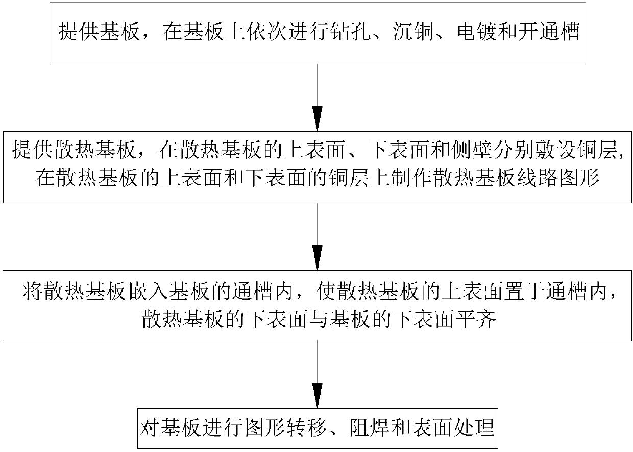
[0030] Such as figure 1 As shown, the present embodiment provides a method for manufacturing a PCB, comprising the following steps:

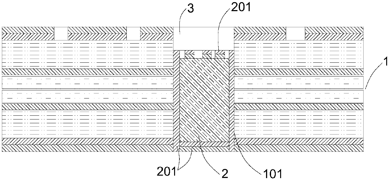
[0031] Step 1: providing a substrate 1 , on which the drilling, copper deposition, electroplating, and opening of the groove 101 are performed in sequence.

[0032] Specifically, the substrate 1 may be a single core board, or a multi-layer board formed by laminating multiple core boards. When the substrate 1 is a multi-layer board formed by lami...


PUM


Abstract

The invention relates to the technical field of circuit board production, and discloses a PCB manufacturing method. The method comprises the following steps that 1, a heat-dissipating substrate and asubstrate with a through groove are provided, the upper surface and side wall of the heat-dissipating substrate are coated with copper layers respectively, and a heat-dissipating substrate circuit pattern is prepared on the copper layer on the upper surface of the heat-dissipating substrate; 2, the heat-dissipating substrate is embedded into the through groove of the substrate, the upper surface of the heat-dissipating substrate is placed in the through groove, and the lower surface of the heat-dissipating substrate is flush with the lower surface of the substrate. According to the PCB manufacturing method and a PCB, the heat-dissipating substrate with the surface lower than the surface of the PCB is embedded in the PCB, the installation space of the PCB is saved, the sidewall metallization of the heat-dissipating substrate is combined with the heat-dissipating substrate surface circuit pattern, and the setting density of power devices on the surface of the heat-dissipating substrate is increased.

Description

technical field [0001] The invention relates to the technical field of circuit board production, in particular to a method for manufacturing a PCB and the PCB. Background technique [0002] Due to the rapid development of electronic technology, PCBs are constantly improving in the direction of miniaturization, multi-function, high integration and high power. Therefore, the requirements for PCB heat dissipation performance are getting higher and higher. The current mainstream PCB heat dissipation technology mainly includes metal substrates. (aluminum substrate, copper substrate) technology, ceramic substrate technology, and buried copper block technology. The heat is dissipated in time, thereby reducing the temperature of electrical appliances and equipment, improving the service life of each high-power component and the working performance and reliability of the entire electrical appliance. [0003] However, the problem with the heat dissipation technology of the above-ment...

Claims


Application Information

Patent Timeline
Patent Type & Authority Applications(China)
IPC IPC(8): H05K1/02H05K1/03
CPCH05K1/0204H05K1/0306
Inventor 李民善肖璐王洪府纪成光袁继旺陈正清
Owner DONGGUAN SHENGYI ELECTRONICS
Why Eureka
Try Eureka