Transient voltage suppressor and method of making the same

A technology for transient voltage suppression and manufacturing methods, applied in the direction of electric solid-state devices, circuits, electrical components, etc., can solve the problems of increasing device manufacturing costs, reducing device performance, and large device area, so as to reduce device manufacturing costs and The effect of small manufacturing cost and small device area

Active Publication Date: 2020-12-22
嘉兴市龙锋市政建设有限公司
View PDF5 Cites 0 Cited by
  • Summary
  • Abstract
  • Description
  • Claims
  • Application Information

AI Technical Summary

Problems solved by technology

However, the additional capacitance introduced by these two structures is large, and the device area is large, which reduces the performance of the device and increases the manufacturing cost of the device.
In particular, the input / output capacitance of a currently commonly used transient voltage suppressor structure is equivalent to the capacitance of a Zener diode, which is prone to have large additional capacitance, large device area, low device performance, and improved device manufacturing. Technical issues such as cost

Method used


Image

  • Transient voltage suppressor and method of making the same
  • Transient voltage suppressor and method of making the same
  • Transient voltage suppressor and method of making the same

Examples


Embodiment Construction

[0035] The following will clearly and completely describe the technical solutions in the embodiments of the present invention. Obviously, the described embodiments are only some of the embodiments of the present invention, rather than all the embodiments. Based on the embodiments of the present invention, all other embodiments obtained by persons of ordinary skill in the art without making creative efforts belong to the protection scope of the present invention.

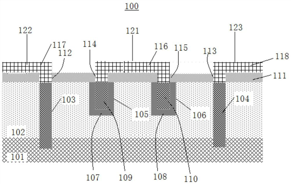
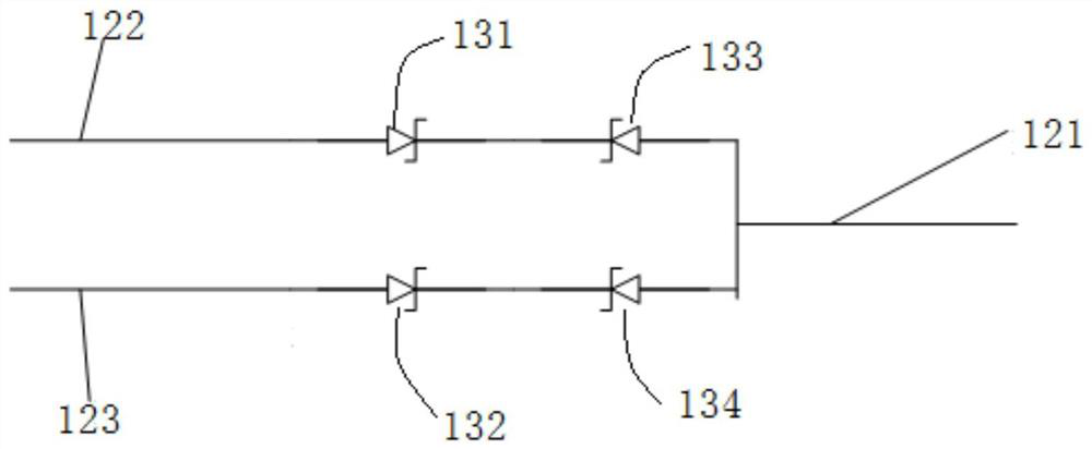
[0036] In order to solve the technical problems of the prior art transient voltage suppressors such as large area, high process difficulty and high device manufacturing cost, the present invention provides an improved transient voltage suppressor, please refer to figure 1 , figure 1 is a schematic structural diagram of the transient voltage suppressor 100 of the present invention. The transient voltage suppressor 100 includes a P-type substrate 101, an N-type epitaxial layer 102 formed on the P-type substrate 101, p...


PUM


Abstract

The invention provides a transient voltage inhibitor and a manufacturing method thereof. The transient voltage inhibitor includes a P type substrate, an N type epitaxial layer formed on the P type substrate, a first P type polysilicon, a second P type polysilicon, a first groove, a second groove, a first N type doped region formed on the inner surface of the first groove, a second N type doped region formed on the inner surface of the second groove, a third P type polysilicon formed on the surface of the first N type doped region in the first groove, and a fourth P type polysilicon formed on the surface of the second N type doped region in the second groove, wherein the first P type polysilicon and the second P type polysilicon penetrate through the N type epitaxial layer and extend to theP type substrate; the first groove and the second groove are formed on the surface, far away from the P type substrate, of the N type epitaxial layer; and the third P type polysilicon is also connected with the fourth P type polysilicon. The transient voltage inhibitor has the advantages of small device area, low process difficulty, low manufacturing cost, and higher protection performance and reliability.

Description

【Technical field】 [0001] The invention relates to the technical field of semiconductor chip manufacturing, in particular to a transient voltage suppressor and a manufacturing method thereof. 【Background technique】 [0002] Transient Voltage Suppressor (TVS) is a solid-state semiconductor device specially designed to protect sensitive semiconductor devices from transient voltage surge damage. It has small clamping coefficient, small size, fast response, and leakage Due to the advantages of small current and high reliability, it has been widely used in voltage transient and surge protection. Electrostatic discharge (ESD), along with other random voltage transients in the form of voltage surges, are commonly found in a variety of electronic devices. As semiconductor devices are increasingly miniaturized, high-density, and multi-functional, electronic devices are increasingly vulnerable to voltage surges, which can even cause fatal injuries. Transient current spikes can be ind...

Claims


Application Information

Patent Timeline
Patent Type & Authority Patents(China)
IPC IPC(8): H01L27/02
CPCH01L27/0255
Inventor 不公告发明人
Owner 嘉兴市龙锋市政建设有限公司
Why Eureka
Try Eureka