Photoetching mask and recovery method for defect of same

A photolithography mask and repair method technology, applied in the field of photolithography mask and photolithography mask defect repair, can solve problems such as mask scrap, avoid imaging problems, improve quality, and improve accuracy and the effect of precision

Inactive Publication Date: 2018-05-25
SEMICON MFG INT (SHANGHAI) CORP +1
View PDF9 Cites 5 Cited by
  • Summary
  • Abstract
  • Description
  • Claims
  • Application Information

AI Technical Summary

Problems solved by technology

Masks with quartz damage out of specification are scrapped, resulting in a mask failure rate of around 0.5%

Method used


Image

  • Photoetching mask and recovery method for defect of same
  • Photoetching mask and recovery method for defect of same
  • Photoetching mask and recovery method for defect of same

Examples


Embodiment 1

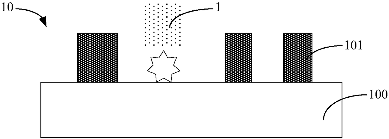
[0043] In order to solve the above-mentioned technical problems, the present invention provides a method for repairing photolithographic mask defects, such as figure 2 As shown, it mainly includes the following steps:

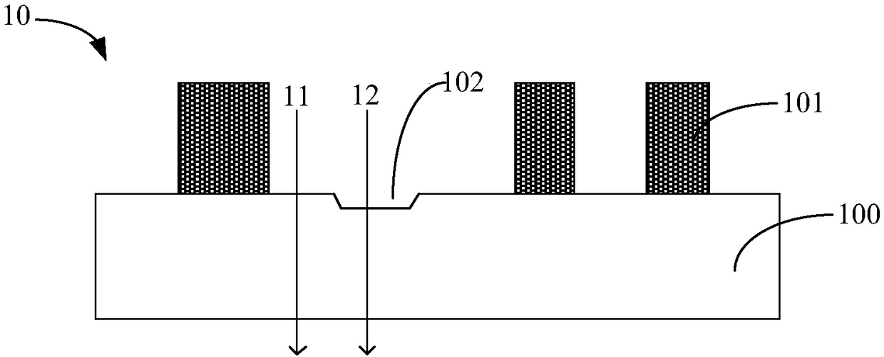
[0044] Step S1: providing a photolithographic mask, the photolithographic mask including a transparent substrate and a light-shielding pattern formed on the surface of the transparent substrate, wherein defective holes are formed on the transparent substrate outside the light-shielding pattern;

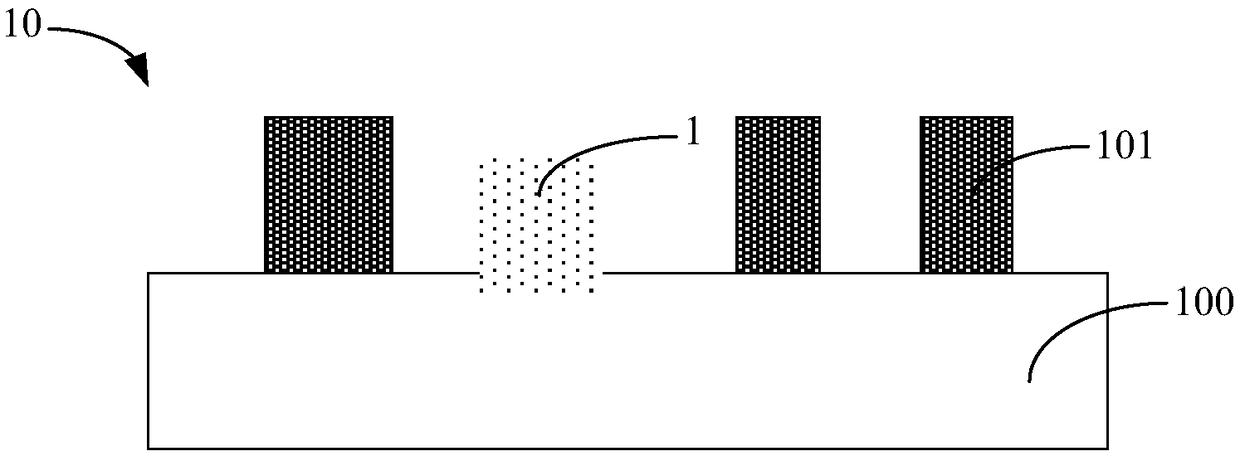
[0045] Step S2: forming a transparent material in the defect hole.

[0046] Through the repairing method of the present invention, a transparent material is formed in the defect hole on the transparent substrate of the photolithography mask, so as to reduce the incident light irradiated into the defect hole and the incident light irradiated on the surface of the transparent substrate outside the defect hole The optical path difference between them, thereby avoiding t...

Embodiment 2

[0072] The present invention also provides a photolithography mask prepared by using the restoration method described in the first embodiment above.

[0073] like Figure 1E As shown, specifically, the photolithography mask 10 includes a transparent substrate 100 and a light-shielding pattern 101 formed on the surface of the transparent substrate 100, wherein defects are formed on the transparent substrate 100 outside the light-shielding pattern 101 A hole in which a transparent material 103 is formed.

[0074] The photolithographic mask plate 10 includes a flat plate with light transmission for exposure light, and at least one light-shielding pattern 101 with light-shielding property for exposure light, which can selectively block the photoresist on the surface of the wafer. Light, and finally form a corresponding pattern on the photoresist on the surface of the wafer.

[0075] The material of the transparent substrate 100 can be any suitable transparent material, among which...


PUM


Abstract

The invention provides a photoetching mask and a recovery method for defect of the same, and relates to the technical field of semiconductors. The recovery method comprises the step of providing the photoetching mask, wherein the photoetching mask comprises a transparent substrate and a shielding pattern, the shielding pattern is formed on a surface of the transparent substrate, a defect hole is formed in the transparent substrate outside the shielding pattern, and a transparent material is formed in the defect hole. By the recovery method, the transparent material is formed in the defect holein the transparent substrate of the photoetching mask, so that the optical path difference between incident light irradiating the defect hole and incident light irradiating the surface of the transparent substrate at an outer side of the defect hole is reduced, the problem of imaging of the defect hole in a wafer is further prevented, the quality of the photoetching mask is improved, the imagingaccuracy and precision of the photoetching mask are improved, and the yield of a semiconductor fabrication process and the performance of the formed device are further improved.

Description

technical field [0001] The invention relates to the technical field of semiconductors, in particular to a photolithographic mask and a method for repairing defects of the photolithographic mask. Background technique [0002] Semiconductor integrated circuits (Integrated Circuit, referred to as IC), that is, semiconductor chips, need to go through multiple processes such as material preparation, plate making, photolithography, cleaning, etching, doping, and chemical mechanical polishing during the manufacturing process. most critical. The lithography process determines the advanced level of the semiconductor chip manufacturing process. It is precisely because of the great progress of the lithography technology that the integrated circuit manufacturing process has been brought from the micron era to the deep submicron era, and then into the nanometer era. The photolithography process requires a complete set (several pieces or up to a dozen pieces) of photoetching mask templat...

Claims


Application Information

Patent Timeline
Patent Type & Authority Applications(China)
IPC IPC(8): G03F1/72
CPCG03F1/72
Inventor 施维
Owner SEMICON MFG INT (SHANGHAI) CORP
Why Eureka
Try Eureka